Multi-channel AND gate ICs for discrete control logic
Packaged AND logic — independent channels, signal levels and input states
A multi-channel AND gate IC combines independent conjunction functions in a shared package. It qualifies combinations of digital control signals before passing a result to the next circuit stage. Choosing the component requires both a Boolean connection plan and compatible electrical levels.
Fixed-function, packaged multi-channel positive-AND gate ICs used in discrete control and qualification logic. The independent gates are connected by the board design; they are distinct from programmable logic arrays, complete priority encoders and the arithmetic circuits on the Full Adder Array and Arithmetic Logic Unit pages.
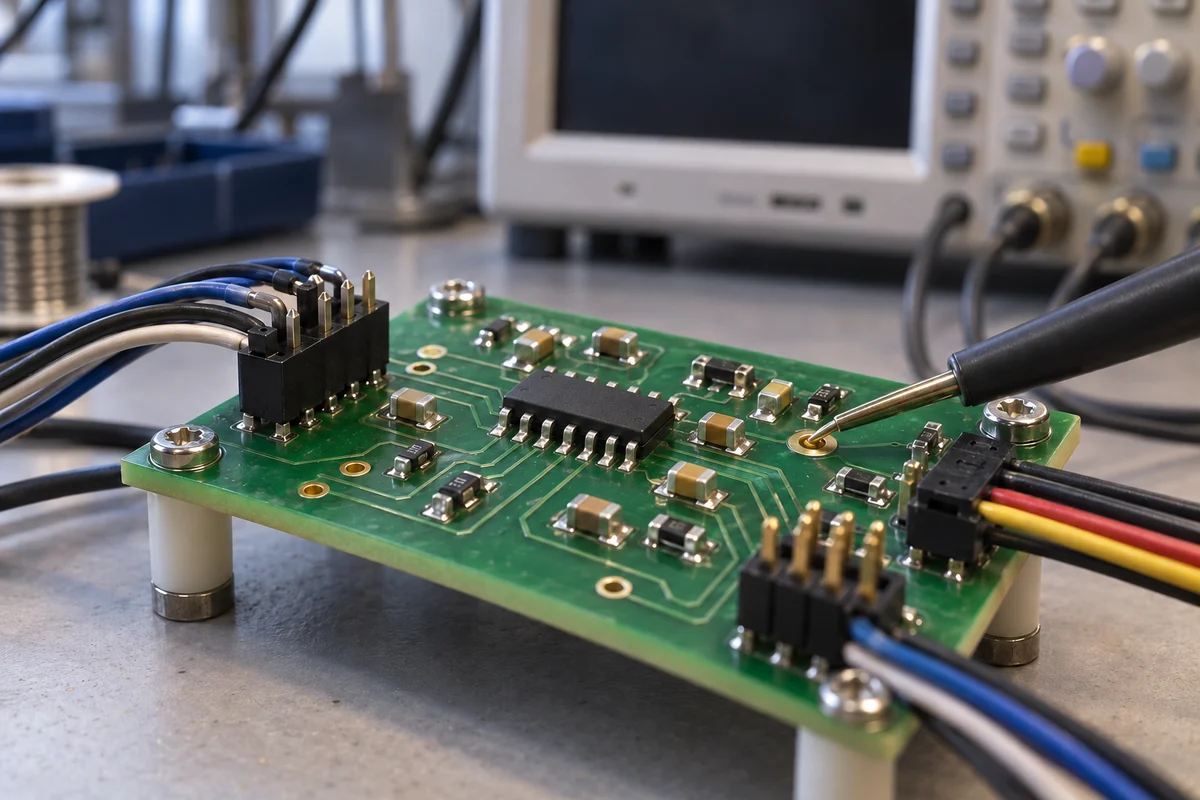
Packaged logic integration on a control-board test bench; the scene illustrates the component setting, with pin connections and electrical limits specified by the selected part’s documentation
Count logic channels separately from inputs per gate
The archived Renesas HD74HC08 sheet describes four independent two-input AND gates. For each gate, the output is HIGH only for the HIGH/HIGH input combination; the other combinations produce LOW. The gate count describes parallel functions, rather than the fan-in of a single function. [1]
Assign each qualification expression to its own gate and map every input and output onto the schematic. If an expression needs more input conditions than a gate provides, specify the chosen wider-input device or the external cascade, including the additional path delay.
Renesas’s archived pin drawing identifies separate A/B/Y connections for the gate channels and shared supply pins in its fourteen-pin arrangement. Match the exact package code, orientation and land pattern when selecting a replacement. [1]
An AND stage evaluates its connected conditions. A priority result requires the surrounding logic to resolve which condition wins. Include that larger circuit separately in the design review and identify the functions assigned to this component.
Check the voltage contract at both sides of each gate
For TI’s SN74HC08 at VCC = 4.5 V, the recommended-input table specifies VIH at least 3.15 V and VIL at most 1.35 V. Compare these input limits with the upstream driver’s guaranteed output levels under its actual load. [2]
The output figures are loaded logic-level guarantees for the named test conditions. Use the receiving device’s thresholds to establish the remaining margin. Keep source current, sink current and shared-package supply limits separate in the component review.
Prepare an input/output connection schedule showing supply rails, driver part numbers, receiving parts, loading and the behaviour of any unpowered circuit. Confirm that the selected logic family is suitable for that schedule; matching a Boolean function alone leaves these electrical requirements unresolved.
SN74HC08 output test
Published limit at VCC = 4.5 V, TA = 25°C, valid VIH/VIL inputs
Give spare inputs a defined state and review slow transitions
TI’s SCBA004E explains how slow input edges combined with supply switching noise can produce output errors or oscillation. It also describes undefined CMOS inputs when a connected driver becomes high impedance, and recommends maintaining valid levels for unused inputs. [3]
Document the state of each input during normal operation, reset, cable removal and upstream power loss. Include spare channels in that schedule and choose their connections using the selected device’s input recommendations.
SCBA004E discusses pull-up and pull-down biasing and cautions that the resulting input transition must meet the device’s limit. Determine the bias network from the actual leakage, loading and timing requirements, rather than treating a spare input as an open connection. [3]
For cascaded AND stages, identify the complete path to the receiving circuit. Obtain propagation-delay limits at the intended supply, temperature and capacitive load, then review changing input conditions as well as settled truth-table states.
The archived Renesas timing circuit includes probe and fixture capacitance in its test load. Account for this loading in the validation setup. [1]
04
AND-gate channel allocation and electrical connection schedule
Paste it into your enquiry below or into an email to a maker, then replace every bracket.
Logic allocation: [independent channel count, inputs per channel and assigned Boolean expressions]
Part/package: [logic family, exact ordering code, package drawing and footprint orientation]
Input sources: [driver parts, supply rails, guaranteed HIGH/LOW levels and transition limits]
Output receivers: [receiving thresholds, source/sink loading and shared-package current budget]
Rest states: [spare inputs, reset, disconnected drivers and upstream power-off behaviour]
Timing review: [cascade path, voltage/temperature/load conditions and fixture capacitance]
Handover: [pin-to-net mapping, connection schedule and recorded logic-level checks]
Explore company information and manufacturing capabilities, then discuss the scope of your project with a relevant supplier.
Share this page
Compiled and source-reviewed by the CNFX editorial team.
Each manufacturer above links to the page on that company's own website where the product is listed, with the date we checked it. How we source and review
· Page last updated 23 October 2026
Buyer questions
Does a quad two-input part act as one wide-input AND gate?
The HD74HC08 archive shows independent channels. Combining more conditions requires an appropriate wider-input part or an explicitly designed external cascade. [1]
Is a Boolean match enough for an electrical replacement?
Check thresholds and loaded output levels. The SN74HC08 tables specify those limits at defined supply and load conditions. [2]
What should happen to spare CMOS inputs?
Assign valid levels according to the device guidance. TI’s input report explains the risks of floating nodes and the need to consider transition time when choosing biasing. [3]
Sources and evidence scope
Sources checked 2026-10-23T19:40:56+08:00. TI’s SCLS081J and input application report provide electrical and input-behaviour references. Renesas’s HD74HC08 Rev.2.00 document is a historical pinout and logic example; it establishes no present availability or approved replacement.