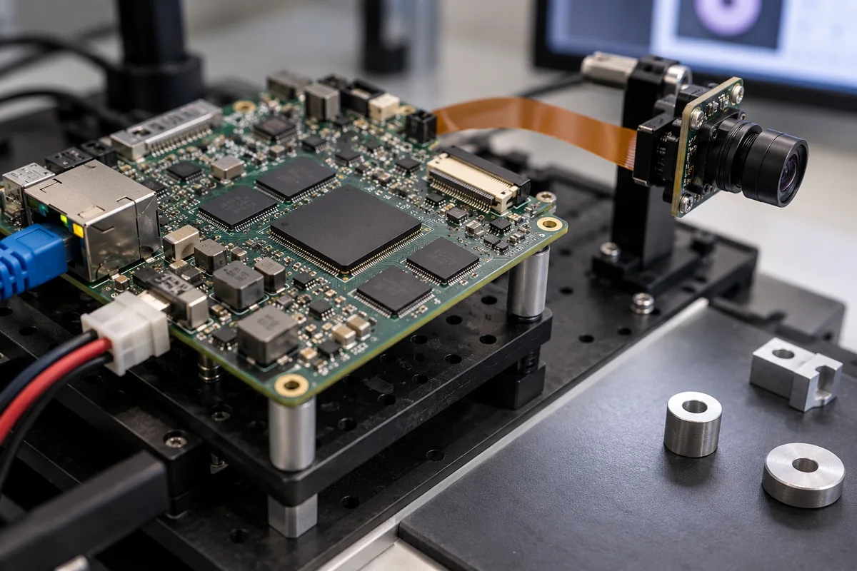
For an endpoint processor, the neural processing unit is one part of the inference path. A usable design must combine the accelerated graph with the CPU work, tensor storage, sensor input and firmware that turn a captured signal into an application decision.
Neural-network acceleration integrated inside an endpoint MCU or SoC, with the processor purchased as a complete device. This page follows model-to-device mapping and memory allocation. Separate accelerator chips and plug-in cards are covered on the Neural processing unit (edge AI accelerator) page; AI M.2 cards and system-on-modules are on the AI accelerator module page. NPU IP licensing and semiconductor fabrication are outside this procurement scope.
Identify the processor that contains the acceleration block
Himax identifies WiseEye2’s HX6538 as an AI microcontroller combining a Cortex-M55 CPU with an Ethos-U55 NPU, sensor interfaces, security functions and power management. Its WiseEye2 solution also includes a separate image sensor. The processor and the complete sensing solution therefore have different delivery boundaries. [1]
State the exact MCU or SoC ordering code and silicon revision in the device enquiry. Identify the sensor and board supplied separately, the application firmware owner and the software package used to access the NPU. Request the device documentation for the selected orderable part rather than treating the acceleration block as a separate packaged component.
The functional breakdown comprises processing cores, a memory/data-transfer interface and execution control. Record which functions belong to the NPU and which are supplied by its surrounding processor and runtime. Their internal material stack and physical implementation are established by the device maker’s documentation; a functional block list is not a chip manufacturing BOM.
02
Read the placement report before committing to the model
Arm’s Vela documentation for version 5.1 and later describes compilation for a selected Ethos-U configuration. Quantized TFLite regions supported by the target become NPU work; unsupported TFLite operations remain for CPU execution. The TOSA path has no CPU fallback. [2]
Retain the input model, quantization settings, conversion tools and compiled artifact as a controlled set. Review the report against the intended device, then assign responsibility for any CPU kernels and application-side transformations. A changed model or compiler version should trigger a fresh placement and accuracy review.
Vela requires the NPU variant/MAC configuration and models platform memory through its system configuration and memory mode. It reports cycle, bandwidth and memory estimates; Arm directs final performance validation to the target hardware. Use those estimates for build comparisons and retain the measured application result separately. [2]
Build evidence
Question it should resolve
Input and converted model identifiers
Which graph, weights, tensor shapes and quantization settings produced the released artifact?
NPU and CPU operator placement
Which parts execute on each engine, and who supplies the required CPU kernels?
Device and compiler configuration
Does the selected accelerator and memory description match the actual processor and software release?
Target measurement record
What are the achieved accuracy, latency, sustained event rate and energy under the application workload?
03
Fit tensor storage and the sensor workload together
Himax’s technical site lists internal 2 MB SRAM and 512 KB TCM for WiseEye2. Those are processor memory resources, not a promise that any model of the same file size fits: include application storage and runtime tensors in the allocation review. The site’s software flow names Vela, TensorFlow Lite for Microcontrollers and CPU fallback through CMSIS-NN or reference kernels. [3]
Obtain a linked memory map and a runtime high-water measurement for the actual application. Account for model constants, intermediate activations, sensor buffers, CPU stacks and the application’s other allocations. Identify which regions are shared or reused, and measure the configuration that will ship.
Define inference timing at the application boundary: input capture, preprocessing, graph execution, postprocessing and the resulting control or communication event. Repeat the workload at the intended sensor rate and power policy, including wake-up and idle periods where they matter. Record the supply measurement boundary so chip power, board power and whole-device energy remain distinguishable.
Device parameter
Record for the selected implementation
Computing power
Published precision and counting convention, plus measured performance for the released graph.
Power consumption
Workload, power policy and measured supply boundary, including active and idle behaviour.
Supply voltage
Selected processor’s core, memory and I/O rails, sequencing and operating limits.
Process node
Maker-declared technology where contractually needed; separate it from measured model efficiency.
Memory bandwidth
Platform memory configuration and measured traffic or contention in the application.
Precision support
Compiler-supported tensor types, quantization configuration and validated accuracy.
Package dimensions
Ordering-code-specific package drawing and PCB assembly requirements.
Weight
Packaged device mass if required by the product’s mechanical budget.
Operating humidity
Equipment environment and package handling/moisture requirements considered separately.
ESD tolerance
Maker’s device-level HBM/CDM qualification; equipment-level protection test specified separately.
MTBF
Supplier reliability evidence and prediction method with stated conditions, when required.
04
Endpoint processor and compiled-model delivery
Paste it into your enquiry below or into an email to a maker, then replace every bracket.
Device: [MCU/SoC order code, revision, integrated NPU configuration and sensor/board delivery split]
Model: [controlled graph and weights, tensor shapes, quantization, accuracy dataset and acceptance target]
Software: [conversion/compiler versions, runtime, CPU kernels, operator placement report and released artifact identifiers]
Memory: [constants, activation arena, sensor buffers, stacks, linked map and runtime peak measurement]
Application: [capture-to-decision timing, sustained input rate, CPU tasks, wake/idle policy and power measurement boundary]
Hardware: [rails/sequencing, package drawing/mass, device operating limits, equipment environment and protection test]
Evidence: [accuracy, target latency/energy, memory headroom, revision control and supplier reliability information]
Discuss the complete MCU or SoC, model deployment and required software release with the chip supplier.
Himax Technologies, Inc.
TBC
Designs and supplies the HX6538 WiseEye2 AI microcontroller with an integrated Cortex-M55 CPU and Ethos-U55 NPU; define the processor and sensor delivery separately.
Explore company information and manufacturing capabilities, then discuss the scope of your project with a relevant supplier.
Share this page
Compiled and source-reviewed by the CNFX editorial team.
Each manufacturer above links to the page on that company's own website where the product is listed, with the date we checked it. How we source and review
· Page last updated 23 October 2026
Buyer questions
Is the WiseEye2 NPU supplied separately from the MCU?
Himax describes HX6538 as the AI microcontroller containing the Cortex-M55 CPU and Ethos-U55 NPU. Order the specified processor or solution and define its delivery boundary. [1]
Does compilation place every operation on the NPU?
Vela’s TFLite path retains unsupported operations for CPU execution. Its TOSA path has no CPU fallback. Inspect the placement for the chosen target and tool version. [2]
Which software accompanies the integrated WiseEye2 accelerator?
Himax’s technical site identifies Vela, TensorFlow Lite for Microcontrollers and a CPU fallback path using CMSIS-NN or reference kernels. Confirm the supplied software versions with the processor vendor. [3]
Sources and evidence scope
Sources checked 2026-10-23T21:27:00+08:00. Original processor and compiler documentation is used for integration boundaries. No latency, efficiency, package or reliability figure is assigned to an unspecified NPU.