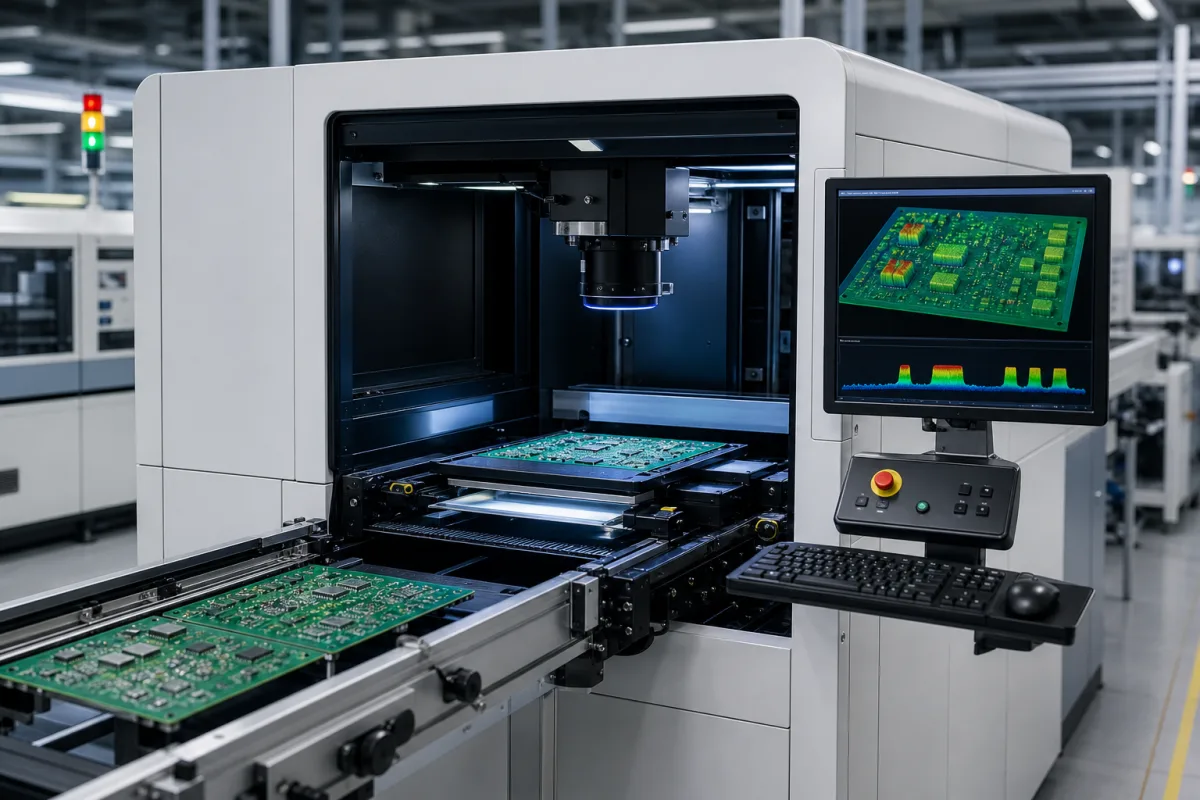
3D SPI after the stencil printer · Measurement principle and shadowing, resolution versus speed, volume accuracy and warp compensation
A solder paste inspection (SPI) system measures paste deposits printed on a circuit board before components are placed, reporting volume, area, height, offset and bridging, so that printing faults can be fixed by washing the board instead of reworking solder joints. Ask three things first: which 3D measurement principle it uses and how it avoids shadowing, what resolution and inspection speed it reaches for your smallest pads and your line takt, and how its accuracy, repeatability and board-warp compensation are specified.
In-line and off-line 3D solder paste inspection machines for SMT lines. Stencil printers, post-reflow automated optical inspection (AOI) and X-ray inspection are outside this page.
CNFX editorial research · Sources checked October 18, 2026 · 5 sources
Test Research Inc. (TRI) explains in its SPI white paper that single-sided laser triangulation projects a laser line and captures images as it moves, needing more images and time for higher resolution, and that with one source the side of a deposit facing away from the laser falls into shadow, so actual paste volume cannot be computed accurately. TRI's own approach projects phase-shifted sinusoidal fringe patterns from two sides with white light while the board is scanned continuously, reconstructing height from four phase maps, and eliminating the shadow effect. [1]
TRI also argues that a paste defect can be fixed in under five minutes by wiping the paste off and reprinting, which is why inspection before placement is more cost-effective than finding defects only at the solder joint. [1] Omron's VP9000 uses the phase-shift method with a 360° ring light to extract the paste outline and stripe patterns from 3D projectors, whose pitch changes with paste height so that height is calculated by triangulation; its standard machine uses dual projectors and its high-speed machine a single projector. [2]
Editorial note: ask how many projection directions the offered machine uses and request a measurement of tall, closely spaced deposits, where shadowing from a single projection angle would show.
Give the supplier the board size and thickness range, smallest aperture and pad pitch, paste deposit heights, line takt time, in-line or off-line, conveyor height and direction, the required volume accuracy and gauge R&R, warp range, feedback link to the printer, data format for traceability, and power supply.
02
Match resolution to speed, and check accuracy and warp
Omron's VP9000 brochure lists digitally switched resolutions of 25/12.5/8.5 µm, 20/10/7 µm or 15/7.5/5 µm. On the standard machine with the 25 µm option, inspection speed is 8,900 mm²/s at standard resolution, 5,600 mm²/s at high and 1,900 mm²/s at super-high resolution. It states volume accuracy within 2% (3σ) on the standard machine and within 3% on the high-speed machine, and PCB warp compensation of ±5 mm, with warp measured and compensated in each field of view. [2]
NeoDen states for its ND S1 a height detection precision of 1 µm and processing time under 0.7 s per frame. Its page also writes “repeatedly (volume, area, height)” as less than 1 µm at 3σ. The dimensional basis for a volume/area repeatability expressed in length units is unclear; ask the maker to identify the metric and test method. [3]
Editorial calculation: assuming a full 330 × 250 mm rectangle is scanned, its area is 82,500 mm². Assuming uninterrupted coverage at the VP9000 standard-machine published area rates, area/rate gives 82,500 ÷ 8,900 ≈ 9.3 s at the 25 µm setting, or 82,500 ÷ 1,900 ≈ 43.4 s at 8.5 µm. This ideal area-rate quotient omits transfer, acceleration, settling, autofocus, programming and processing overhead; it is not a maker-published or measured board cycle time. [2]
03
Put speed, camera and warp figures from three makers side by side
Koh Young describes its "KY8030-3" as using 3D dual-inspection technology "to eliminate critical shadow problems", with an inspection speed of 91.2 cm²/sec, and says the latest options make it twice as fast as its predecessor. Its warp compensation, called Z-tracking 3D Compensation, calculates and detects substrate warpage. [4]
MIRTEC’s current Korean MS-11 page has a 25MP camera label in its upper feature panel, while the detailed camera paragraph states 15MP with 10µm/15µm lenses and CoaXPress transfer. Both statements are present; ask MIRTEC to confirm the ordered camera/configuration. The detailed page also states Z-axis compensation of PCB warp up to ±5 mm within the field of view. [5] Omron gives ±5 mm for the VP9000 [2]; obtain the board-specific height-reference method from each supplier.
The speed figures are not stated at matching conditions. Koh Young gives one figure without a resolution on the page reviewed [4], while Omron's falls from 8,900 to 1,900 mm²/s as resolution rises [2]. TRI explains that single-sided projection leaves part of a deposit in shadow so paste volume cannot be computed accurately [1]. Ask each supplier for speed at the resolution you need, with the number of projection directions used.
The published speed values have different measurement conditions. Retain each maker’s speed with its resolution and projection configuration, and obtain a board-specific cycle measurement before comparing throughput. [4][2]
Dual projectors (standard machine); single projector (high-speed machine) [2]
Koh Young does not specify the speed-resolution pairing on the reviewed page. MIRTEC’s upper feature panel and detailed camera paragraph differ; confirm the selected configuration with the maker. [4][5]
04
In-line and off-line SPI equipment listed by the suppliers
NeoDen lists its ND S1 SPI machine, while Reaching EA lists in-line and off-line SPI equipment. Define conveyor integration, measurement configuration and printer feedback with the selected machine. [3]
05
Fringe projectors, imaging optics and the board-height reference
2 companies list this product among what they make. Company figures are quoted from each
company's own website; every card states where the relationship came from.
Zhejiang NeoDen Technology Co., Ltd
TBC
Lists the ND S1 3D solder paste inspection machine with printers, placement machines and reflow ovens.
Explore company information and manufacturing capabilities, then discuss the scope of your project with a relevant supplier.
Share this page
Compiled and source-reviewed by the CNFX editorial team.
Each manufacturer above links to the page on that company's own website where the product is listed, with the date we checked it. How we source and review
· Page last updated 13 October 2026
Buyer questions
Why does a 3D SPI need projection from more than one side?
TRI explains that single-sided measurement leaves the far side of a deposit in shadow, so volume cannot be computed accurately; dual-sided projection removes the shadow. [1]
Does higher SPI resolution slow inspection?
Yes; Omron's VP9000 falls from 8,900 mm²/s at 25 µm to 1,900 mm²/s at 8.5 µm on its standard machine. [2]
How much board warp can an SPI compensate?
Omron's VP9000 states ±5 mm, compensated in each field of view. [2]
How fast is a 3D solder paste inspection machine?
Koh Young states 91.2 cm²/sec for its KY8030-3; Omron states 8,900 mm²/s (89 cm²/s) for the VP9000 at its 25 µm standard resolution, falling to 1,900 mm²/s at super-high resolution. Ask for speed at the resolution you need. [4][2]
Sources and what still needs a direct check
Sources checked 2026-10-18. TRI, Omron and NeoDen describe their own SPI machines and methods; accuracy figures are stated under each maker's conditions.