Editorial Technical Reference

Automated Printed Circuit Board (PCB) Optical Inspection System

This page explains how Automated Printed Circuit Board (PCB) Optical Inspection System is classified within Manufacture of Consumer Electronics. Technical values and manufacturer relationships are research references; confirm the current specification and supplier evidence for each order.

Technical Definition & Core Assembly

Automated vision system for detecting defects on PCBs during consumer electronics manufacturing.
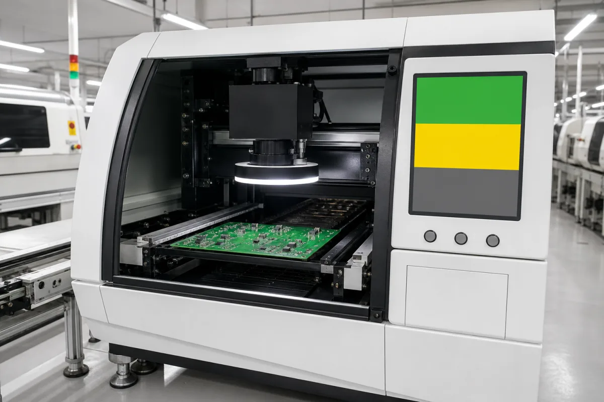
Automated Printed Circuit Board (PCB) Optical Inspection System in a manufacturing environment
Representative product image. Confirm appearance and specifications with the manufacturer.

Product Specifications

Technical details and manufacturing context for Automated Printed Circuit Board (PCB) Optical Inspection System

Definition
This industrial-grade automated optical inspection (AOI) system is designed for quality control in consumer electronics PCB assembly lines. It uses high-resolution cameras and advanced image processing algorithms to identify manufacturing defects such as solder bridges, missing components, misalignment, and surface imperfections. The system plays a critical role in B2B supply chains by ensuring product reliability before final assembly, reducing rework costs, and maintaining consistent quality standards across high-volume production environments. Manufacturers integrate these systems to meet stringent quality requirements for televisions, audio equipment, and home entertainment devices.

The system features a robust construction with an aluminum alloy frame, tempered glass windows, and stainless steel components. It offers an inspection resolution of 10–20 μm/pixel, supporting PCBs up to 510×460 mm. Inspection speed ranges from 0.5 to 2.0 cm²/sec, with camera resolutions from 5 to 20 megapixels. Lighting options include LED, UV, and IR configurations. The false call rate is 0.5–2.0%, and detection accuracy is ±0.05 mm. Operating temperature is 10–40 °C, relative humidity 20–80% RH (non-condensing), and power supply is 220 V AC ±10% (single phase, 50/60 Hz). Power consumption is 1.5–3.0 kW, machine weight 800–1200 kg, and footprint 1500×1200×1800 mm. The system detects common defects such as missing, misaligned, and bridging components, as well as solder and trace issues.

All listed values are reference ranges; verify model-specific specifications and applicable standards with the legal manufacturer or supplier before procurement or use.
Working Principle
High-resolution cameras capture images of PCBs under controlled lighting. These images are then analyzed by computer vision algorithms that compare actual board features against reference designs to detect deviations and defects. The system uses multiple lighting types (LED, UV, IR) to enhance contrast for different defect types. The inspection process is automated, providing consistent and repeatable results. The system's detection accuracy and false call rate are influenced by the chosen resolution, lighting configuration, and the complexity of the PCB design. Operators should calibrate the system according to the specific board types and quality requirements.
Common Materials
Aluminum Alloy Frame, Tempered Glass Windows, Stainless Steel Components
Technical Parameters
ParameterTypical rangeNotes & selection driver
Inspection ResolutionRequired10–20 μm/pixelMinimum detectable defect size
Maximum PCB SizeRequired510×460 mmLargest board dimension supported
Inspection SpeedRequired0.5–2.0 cm²/secArea inspection rate
Camera ResolutionRequired5–20 megapixelsImaging sensor resolution
Lighting TypesLED, UV, IR countNumber of programmable lighting configurations
False Call RateRequired0.5–2.0 %Percentage of false defect detections
Operating Temperature10–40 °COutside range may affect accuracy.
Relative Humidity20–80 %RHNon-condensing; high humidity may cause fogging.
Power Supply220 ±10% V ACSingle phase, 50/60 Hz.
Power Consumption1.5–3.0 kWDepends on lighting and computer configuration.
Machine Weight800–1200 kgHeavier machines may require reinforced flooring.
Footprint (L×W×H)1500×1200×1800 mmSpace required for installation and maintenance.
Detection Accuracy±0.05 mmPositional accuracy of defect location.
Defect TypesSolder, trace, componentCommon defects: missing, misaligned, bridging.

Ranges are indicative industry figures for RFQ preparation, not a supplier commitment. Confirm every value and standard with the legal manufacturer before ordering.

Components / BOM

Industry Taxonomies & Aliases

Commonly used trade names and technical identifiers for Automated Printed Circuit Board (PCB) Optical Inspection System.

Industrial Ecosystem & Supply Chain Structure

Complementary Systems
Downstream Applications
Specialized Tooling

Application Fit & Sizing Matrix

Operational Limits
pressure: Atmospheric (no pressure requirements)
other spec: Humidity: 30-70% RH non-condensing, Vibration: <0.5G, Illumination: Controlled ambient light
temperature: 15-35°C (operating), 0-50°C (storage)
Media Compatibility
✓ FR-4 PCB substrates ✓ Solder mask coatings (LPI, dry film) ✓ Surface mount components (0201 to large BGAs)
Unsuitable: High-reflectivity metallic surfaces without matte finish
Sizing Data Required
  • Maximum PCB dimensions (length x width)
  • Minimum defect size to detect (in microns)
  • Required inspection speed (boards per hour)

Reliability & Engineering Risk Analysis

Failure Mode & Root Cause
Optical System Degradation
Cause: Accumulation of dust, debris, or contaminants on lenses, mirrors, or sensors, leading to reduced image clarity, false positives/negatives, and calibration drift due to environmental exposure and inadequate filtration.
Mechanical Positioning Inaccuracy
Cause: Wear or misalignment in linear guides, belts, or servo motors from repeated high-speed movements, vibration, or lack of lubrication, causing positional errors that affect inspection accuracy and throughput.
Maintenance Indicators
  • Increasing frequency of false defect detections or missed defects during inspection runs
  • Unusual audible vibrations, grinding noises, or inconsistent movement from the conveyance or positioning mechanisms
Engineering Tips
  • Implement a preventive maintenance schedule for cleaning optical components with approved materials and recalibrating the system using master calibration boards to ensure consistent performance.
  • Regularly monitor and log positional accuracy metrics, and perform alignment checks and lubrication of mechanical components as per manufacturer specifications to prevent drift and wear.

Indicative industry ranges for design and RFQ preparation. Confirm the exact figures and applicable standard with the manufacturer before specifying.

Compliance & Manufacturing Standards

Applicable Standards
ANSI/IPC-A-610 - Acceptability of Electronic Assemblies CE Marking - Directive 2014/35/EU (Low Voltage Directive)

Quoted from the published standard.

Manufacturing Precision
  • Component Placement Accuracy: +/-0.05mm
  • Solder Joint Inspection Resolution: 0.01mm
Quality Inspection
  • Automated Optical Inspection (AOI) - Defect Detection
  • Electrical Test - Continuity and Isolation Verification

Manufacturers of Automated Printed Circuit Board (PCB) Optical Inspection System

Manufacturer profiles associated with Automated Printed Circuit Board (PCB) Optical Inspection System.

Sourcing Automated Printed Circuit Board (PCB) Optical Inspection System from China?
Tell us your specification and target quantity — we will match it against manufacturer records and come back with the factories that fit.
Request manufacturers We manufacture this

Manufacturer listings support early research and capability understanding. They are not certification, ranking, or transaction guarantees.

Share this page
Technical documentation
Request current drawings, revision history, and a signed specification sheet.
Manufacturing capability
Verify equipment lists, process limits, capacity, and representative production evidence.
Inspection readiness
Confirm test methods, calibrated equipment, sampling plans, and traceable reports.
Supplier transparency
Check the legal entity, factory address, ownership, certifications, and direct contacts.

CNFX does not score or rank suppliers. Buyers must verify all claims and documents with the legal manufacturer before ordering.

Frequently Asked Questions

What types of defects can this AOI system detect?

The system detects common manufacturing defects such as missing components, misaligned parts, solder bridges, and surface imperfections. It also identifies issues with solder joints and PCB traces. The specific defect types are listed as solder, trace, and component defects.

What is the maximum PCB size that can be inspected?

The maximum PCB size supported is 510×460 mm. Boards larger than this may not be accommodated. Verify the exact dimensions with the manufacturer for your specific application.

What are the environmental requirements for operation?

The system operates in temperatures from 10 to 40 °C and relative humidity from 20% to 80% RH (non-condensing). High humidity may cause fogging, and operating outside these ranges may affect accuracy. Ensure the installation environment meets these conditions.

How accurate is the defect location?

The detection accuracy is ±0.05 mm, meaning the system can pinpoint defect locations with high precision. However, actual performance may vary based on the inspection resolution, lighting, and PCB complexity. Confirm with the manufacturer for your specific setup.

Data Basis

Editorial classification, named public sources where available, and source-reviewed manufacturer records.

Preliminary Technical Classification
This page supports structured research, RFQ preparation, and supplier evaluation. It does not replace buyer-led supplier qualification, standards review, or technical approval.
Buyer enquiry

Request manufacturing insight for Automated Printed Circuit Board (PCB) Optical Inspection System

Ask for use case, specification boundaries, supplier type, and RFQ preparation information for this product.

Where it goes
Straight to the CNFX editorial desk, and to the manufacturer if this product is linked to a claimed profile. Nothing is broadcast to a supplier list.
Your details stay here
We do not sell or rent enquiry data, and we do not add you to a mailing list. Used only to answer this request.
No commission, no middleman
CNFX is a directory. We take no cut of any order and never negotiate on a supplier's behalf.
What we don't claim
A listing is not an endorsement. Qualify every supplier and verify every figure yourself before ordering.

Your business information is used only to process this request.

Thank you! Your message has been sent. We'll respond within 1–3 business days.
Sorry, we couldn't send your message. Please try again, or email us at [email protected].

Need to Manufacture Automated Printed Circuit Board (PCB) Optical Inspection System?

Compare manufacturer profiles with relevant product and process capability.

Previous Product
Digital Audio Signal Processor Module
Last Product
Get QuotesChat