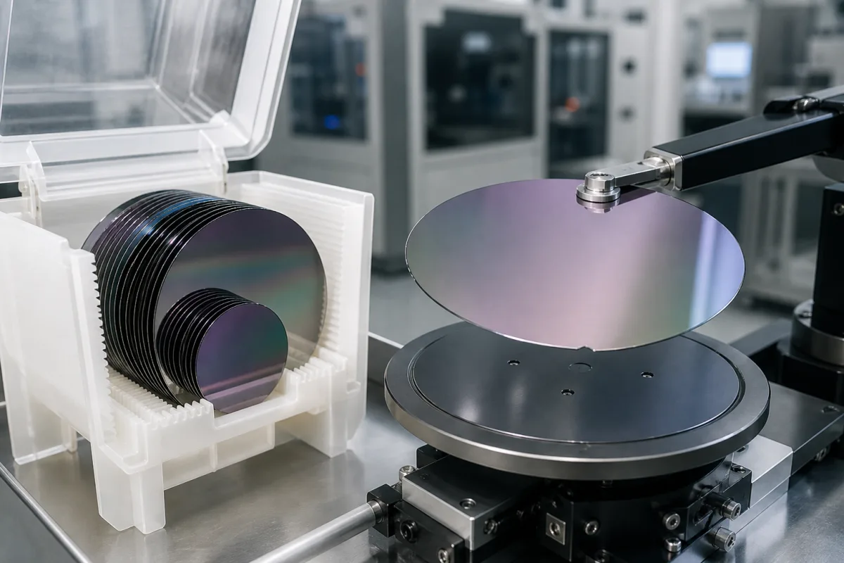
Silicon substrates · Diameter, thickness, flats and notch; TTV, bow and warp; orientation, polish and resistivity
A silicon wafer substrate is a thin, polished disc sliced from a single-crystal silicon ingot, doped to a chosen type and resistivity, on which devices, MEMS or thin films are built. Ask three things first: diameter, thickness and the flat or notch standard your tools expect; the flatness figures (TTV, bow, warp) and surface finish; and crystal orientation, dopant type and resistivity range.
Monocrystalline silicon wafers (prime, test and dummy grades), single- or double-side polished, with or without oxide. Silicon-on-insulator, epitaxial and compound semiconductor wafers, solar cells and wafer processing services are outside this page.
CNFX editorial research · Sources checked October 11, 2026 · 4 sources
TopLine's wafer dimension drawing lists diameters and thicknesses from 2 in to 300 mm: 100 mm ± 0.5 mm at 525 ± 20 µm, 125 mm ± 0.5 mm at 625 ± 20 µm, 150 mm ± 0.2 mm at 675 ± 20 µm (or 625 ± 15 µm), 200 mm ± 0.2 mm at 725 ± 20 µm and 300 mm ± 0.2 mm at 775 ± 20 µm. Wafers up to 150 mm carry a primary flat (32.5 mm at 100 mm, 57.5 mm at 150 mm) and a secondary flat at 45°, 90° or 180° from it, while 200 and 300 mm wafers carry a notch. [1]
MicroChemicals gives similar typical thicknesses, about 525 µm for 4 in, 675 µm for 6 in and 725 µm for 8 in, set by mechanical stability, and says thickness tolerance over a batch "is usually specified as +/- 25 μm", with measured values "often around +/- 15 μm". It notes that makers may set a minimum thickness of about 200 µm because of breakage during grinding and polishing. [2]
Editorial calculation: a 300 mm wafer has 2.25 times the area of a 200 mm wafer ((300/200)²), while its nominal thickness rises only from 725 to 775 µm. [1]
Give the supplier the diameter, thickness and tolerance, flat or notch standard, grade (prime, test, dummy), orientation, dopant type and resistivity range, polish (SSP or DSP), TTV, bow and warp limits, particle and metal limits, oxide or other films, quantity and packaging (cassette type, cleanroom bagging).
02
Specify flatness, surface, orientation and resistivity
MicroChemicals defines total thickness variation (TTV) as the maximum difference between the thickest and thinnest points of a wafer, bow as the maximum deviation of the median surface from a reference plane, and warp as that deviation after overall bending is corrected. Up to 4 in it says wafers "are usually specified to TTV < 10 μm" (below 5 µm achievable without great effort), bow below 40 µm and warp below 40 µm, with achievable values rising for larger diameters. [2]
It states that polished surfaces have roughness around 1 nm RMS (about 0.5 nm feasible), unpolished sides a few µm; orientation such as <100>, <110> or <111> has tolerances that "are usually +/- 0.5°"; and because dopant concentration varies axially and radially, resistivity is specified as a range that "typically lies within an order of magnitude" (for example 1–10 Ω·cm), or a factor of about two with tighter processes and sorting. Below about 10¹⁶ cm⁻³ dopant concentration, resistivity falls roughly in inverse proportion to concentration; above it, mobility falls and the curve flattens. [2]
Editorial calculation: in the inverse-proportion region, doubling the dopant concentration roughly halves the resistivity, so a 1–10 Ω·cm range corresponds to about a tenfold spread in dopant concentration. [2]
03
Allow for film stress changing bow and warp after deposition
A 2025 Sensors paper led by Southeast University (Nanjing) measured warp and film stress on silicon wafers by phase-measuring deflectometry and checked it against an industrial stress tool (Toho FLX-2320-S). Its test wafer was an 8-inch silicon wafer 0.725 mm thick, with substrate modulus Es = 169 GPa and Poisson's ratio 0.25, coated with a 620 nm tungsten film; stress follows from the change in curvature through the Stoney equation, σ = Es·ts² / (6(1 − νs)·tf·R). [4]
The authors note that the FLX tool gives stress only along the two median lines it scans, while the full-field method also resolved changes in curvature at the wafer edge. The 0.725 mm thickness matches the 725 µm nominal listed for 200 mm wafers on the TopLine drawing. [4][1]
Editorial calculation: rearranging the Stoney equation with the paper's values (169 GPa, 0.25, 0.725 mm, 620 nm, 230.5 MPa) gives a radius of curvature of about 138 m, and a sag of about 36 µm across a 200 mm wafer (r² / 2R with r = 100 mm). That is close to the 40 µm bow limit MicroChemicals quotes for wafers up to 4 in, so if your process deposits stressed films, give the supplier the bow and warp limits you need after deposition, not only as-shipped values. [4][2]
Item (Southeast University study)
Value
Wafer
8-inch Si, 0.725 mm thick; Es 169 GPa; νs 0.25 [4]
Suppliers linked to this page list silicon wafers; each card links to the page reviewed.
Listings include silicon wafers among crystal wafers and substrates and optical materials.
05
Order against SEMI M1 and name the test method for each property
SEMI's M1 specification standardises silicon wafer dimensions so that the same processing equipment can be used across fabrication lines; the current revision listed by SEMI is M1-0924. [3] Its abstract says it covers ordering information and requirements for electronic-grade, single crystal polished wafers, applies specifically to prime wafers with at least one chem-mechanically polished surface, and does not cover ground, lapped or unpolished wafers, though it may guide their procurement. [3] It also states that its thickness, TTV, bow and warp values apply only before back-surface films, extrinsic gettering or other thermal treatments, so confirm when the supplier measures these on coated wafers. [3]
The abstract points to separate SEMI documents for neighbouring grades: test wafers (SEMI M8), premium wafers (SEMI M24), reclaimed wafers (SEMI M38) and epitaxial wafers (SEMI M62). It uses U.S. customary units for 2 inch and 3 inch wafers and SI units for 100 mm and larger, and includes guides for 300 and 450 mm prime wafers for the 32, 22 and 16 nm technology generations. [3]
Fill the specification fields with values for your wafers
A wafer quotation needs values for your process. The table explains each field, gives published values where a reviewed source states them, and says what to obtain from the supplier.
Explore company information and manufacturing capabilities, then discuss the scope of your project with a relevant supplier.
Share this page
Compiled and source-reviewed by the CNFX editorial team.
Published product pages show what a company offers, not tested performance. Confirm the legal seller, factory and scope for your order. How we source and review
· Page last updated 13 October 2026
Buyer questions
How thick is a standard silicon wafer?
A wafer dimension drawing lists 525 ± 20 µm for 100 mm, 675 ± 20 µm for 150 mm, 725 ± 20 µm for 200 mm and 775 ± 20 µm for 300 mm. [1]
What are TTV, bow and warp?
TTV is the thickest-minus-thinnest point; bow is the median surface's maximum deviation from a reference plane; warp is that deviation after overall bending is corrected. [2]
Why is resistivity given as a range?
Because dopant concentration varies along and across the crystal; MicroChemicals cites about one decade, such as 1–10 Ω·cm. [2]
Which standard defines prime polished silicon wafer dimensions?
SEMI M1, Specification for Polished Single Crystal Silicon Wafers (current revision M1-0924 per SEMI), which covers ordering information and dimensional requirements for prime wafers with at least one chem-mechanically polished surface. [3]
How much can a deposited film bend a silicon wafer?
In a Southeast University study, a 620 nm tungsten film on a 0.725 mm, 8-inch wafer carried about 206–243 MPa of stress; by the Stoney equation that is a radius of about 138 m, or roughly 36 µm of sag across 200 mm (editorial calculation). [4]
Sources and what still needs a direct check
Sources checked 2026-10-11. TopLine is a maker of dummy components publishing a dimension drawing; MicroChemicals is a wafer and chemicals supplier describing typical specifications. SEMI standards govern formal wafer specifications. A Southeast University study reports measured film stress and warp on an 8-inch silicon wafer.