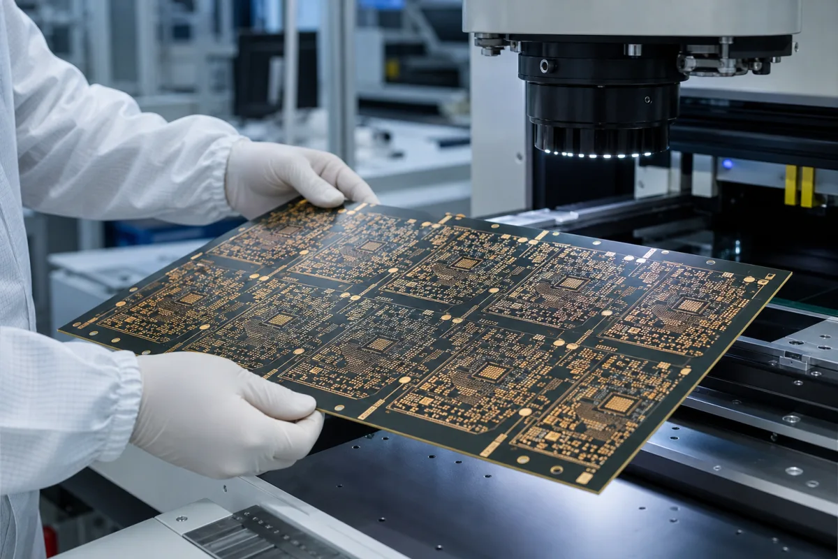
HDI PCB substrate of the substrate-like (SLP) type: board-size HDI built by mSAP for lines of 30/30 µm and below
Board-size HDI made with package-substrate methods · modified semi-additive (mSAP) copper on ultra-thin carrier foil, 30/30 µm and finer lines, and the copper that is plated and etched back on each layer
A conventional HDI board is made by etching away copper that is not wanted. At around 30 µm line and 30 µm space that stops working at production yields, so the boards inside high-end phones moved to the method package-substrate makers use: start from a very thin copper layer, plate the circuit up through a resist pattern, then remove the thin starting copper. The product is still a board in size and function, but its line widths, copper foils and plating steps belong to the substrate world. Buyers who need it have to specify those process details, which ordinary HDI orders leave to the fabricator.
Substrate-like printed circuit boards (SLP): board-size HDI constructions built with the modified semi-additive process (mSAP or amSAP) on copper-clad laminate or carrier-supported ultra-thin copper foil, for line and space from about 30/30 µm down to 20/20 µm, as used for smartphone and other compact mainboards. HDI boards made by subtractive etching, with their IPC-2226 construction types, microvia stacking and 1+N+1 build-ups, are covered on the HDI PCB page; BT and ABF package substrates for BGA and flip-chip on the IC substrate (package substrate) page; conventional rigid multilayer boards on the Multilayer PCB page.
CNFX editorial research · Sources checked October 12, 2026 · 3 sources
Between 35/35 µm subtractive HDI and 10/10 µm package substrate: the line-and-space band SLP occupies
DuPont gives the line/space used in mass-produced smartphone HDI boards as 35/35 µm and says the target was moving to 30/30 µm, which it states cannot be reached by traditional subtractive processes with high enough yields for volume production. It notes that the semi-additive process (SAP) used for package substrates can reach 10/10 µm or even 8/8 µm, but would require HDI makers to buy new equipment and adopt a new dielectric, Ajinomoto Build-up Film; mSAP instead starts from copper-clad laminate, thin copper or a copper-reduction step, which is why boards made this way are called substrate-like PCBs. [1]
Yole Développement, as reported by 3D InCites in 2018, places the board-versus-package-substrate competition zone between L/S 30/30 µm and 20/20 µm, describes SLP as a large substrate manufactured in mSAP in the size and function of a board, and lists higher line resolution, better electrical performance and potential space and energy savings as its benefits over standard or HDI boards. Its analysts also note that, although mSAP is mature for package substrates, considerable challenges remained in making substrates at PCB size. [2]
Editorial calculation: a line and space of 35/35 µm gives a 70 µm pitch, about 14.3 traces per millimetre of routing width; 30/30 µm gives a 60 µm pitch, about 16.7 per millimetre, and 20/20 µm a 40 µm pitch, 25 per millimetre. [1][2]
State the minimum line and space on each layer, which layers need it, and the process the fabricator will use to reach it (subtractive, mSAP or amSAP); ask for yield or capability data at that line width rather than a single headline figure.
02
3 µm base, 28 µm plated, 8 µm etched back: how much copper each SLP generation removes
DuPont describes the first-generation SLP process in the iPhone 8 and X as starting from a 3 µm copper base, adding 0.4 µm of electroless copper and 5 µm of flash copper, then 18 to 22 µm of via-fill copper for a total of 28 µm, and reaching the final 20 µm by a complicated etch that removes the extra 8 µm. It says plating extra copper and etching it back raises the possibility of technical and reliability issues and adds cost. [1]
Two second-generation routes are described. Advanced mSAP (amSAP) drops the flash copper and plates thick electroless copper to 1.6 µm, followed by 18 to 22 µm of fill, still needing a 5 µm etch to reach 20 µm. The electroless-plus-flash (ELF) process the blog credits to Qnity deposits 0.1 µm and 0.9 µm in one step followed by 16 to 18 µm of fill, giving about 20 µm with no etch-back. [1]
Editorial calculation from the layer values: the first-generation stack adds up to 26.4 to 30.4 µm across the 18–22 µm fill range (28 µm at the 20 µm midpoint, matching DuPont's figure), and amSAP to 19.6 to 23.6 µm before etching. The ELF layers add up to 17 to 19 µm, slightly below the about 20 µm DuPont states, so ask the supplier for the measured final thickness. [1]
The thin starting copper is a purchased material. Mitsui Kinzoku describes its MicroThin series as 1.5 to 5 µm copper foil carried on an 18 µm or 12 µm carrier foil through a release layer, designed for mSAP; the carrier is peeled off after lamination. It lists four grades by roughness and target line/space by mSAP: MT18SD-H at Rz 3.0 µm for 30/30 µm, MT18Ex at Rz 2.0 µm for 25/25 µm, MT18FL at Rz 1.3 µm for 15/15 µm and MT18GN at Rz 0.9 µm for 10/10 µm, and names smartphone motherboards and package substrates as applications. [3]
Ask which mSAP route the fabricator runs, the base copper foil (thickness, carrier and roughness grade), the final copper thickness after any etch-back, and how it measures line width after the flash etch.
03
Line, copper and process data for a substrate-like PCB
Paste it into your enquiry below or into an email to a maker, then replace every bracket.
Line and space: [minimum per layer; which layers]
Process: [mSAP; amSAP; other]
Base copper: [foil thickness; carrier; roughness grade]
Final copper: [thickness after etch-back; tolerance]
Construction: [layer count; any-layer or build-up; via fill]
Dielectric: [material; thickness]
Panel and array: [panel size; units per panel]
Inspection: [line-width measurement; AOI; electrical test]
Explore company information and manufacturing capabilities, then discuss the scope of your project with a relevant supplier.
Share this page
Compiled and source-reviewed by the CNFX editorial team.
Each manufacturer above links to the page on that company's own website where the product is listed, with the date we checked it. How we source and review
· Page last updated 13 October 2026
Buyer questions
What is a substrate-like PCB?
A board-size HDI made with the modified semi-additive process used for package substrates, aimed at line and space of 30/30 µm and below. [1][2]
Why can't ordinary HDI reach 30/30 µm?
DuPont states that 30/30 µm cannot be achieved by traditional subtractive processes with high enough yields for volume manufacturing. [1]
How thin is the copper foil used for mSAP?
Mitsui Kinzoku's MicroThin foils are 1.5 to 5 µm on an 18 or 12 µm carrier, in grades targeting 30/30 down to 10/10 µm. [3]
Why does first-generation SLP etch copper back?
Per DuPont, it plates to about 28 µm and must etch about 8 µm away to reach 20 µm; newer processes reduce or remove this step. [1]
Sources and what still needs a direct check
Sources checked 2026-10-12. Process figures come from a DuPont electronics blog on SLP metallization; the line-and-space roadmap from Yole Développement as published by 3D InCites; copper foil grades from Mitsui Kinzoku's MicroThin product page.