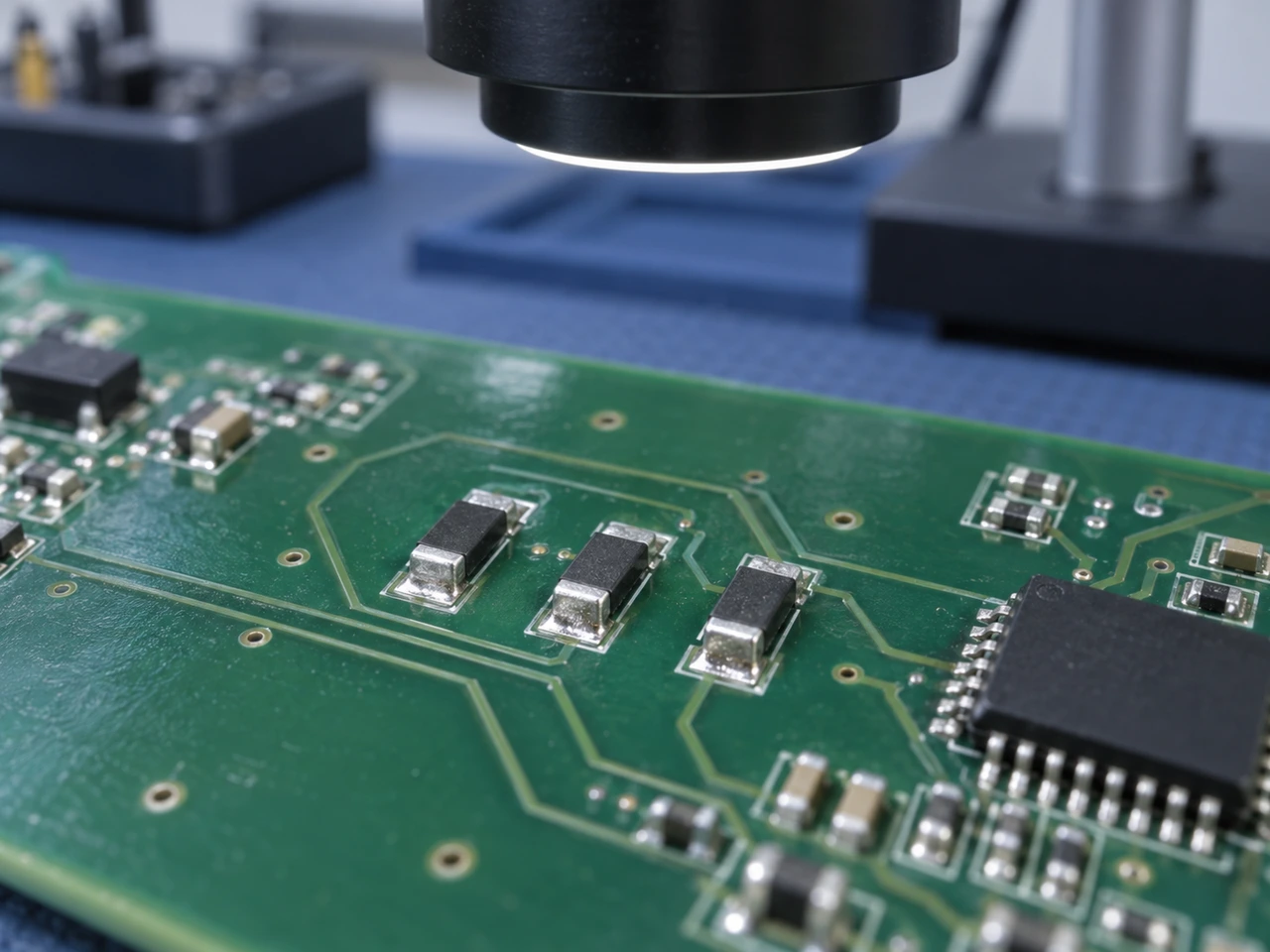
A BOM line reading “0603, 10 kΩ, 1%” leaves the power mode, temperature drift, termination finish and assembly requirements unresolved. Start with the circuit duty, then identify the exact series and ordering code.
For fixed surface-mount resistors on circuit boards. The worked reference is Vishay D/CRCW e3 thick film; specialist RF and high-temperature supplier examples have their own construction and limits. This is not a universal chip-resistor specification.
CNFX editorial research · Sources checked October 10, 2026 · 5 sources
Choose the power mode together with the allowed resistance drift
Vishay’s D/CRCW e3 datasheet, revision 14 April 2026, gives a larger dissipation figure on its first page than the standard-mode figure for some sizes. Page 2 explains the difference. An apparent upgrade in watts can also change the permitted long-term resistance change. Keep these columns together when comparing quotations. [1]
At the stated rated conditions: ≤1% change after 1,000 h; ≤2% after 8,000 h
≤2% after 1,000 h; the 8,000 h cell is blank. That blank is not an 8,000 h guarantee. [1]
Leave room for heat from the board
Power in the resistance film raises its temperature above the local ambient. Vishay limits the film temperature to 155°C and makes permissible dissipation depend on the assembled part and PCB. The category temperature range is not permission to dissipate the full 70°C rating everywhere in that range. [1]
For a 0603 in standard mode, the published linear derating curve falls from 0.10 W at 70°C to zero at 155°C. At 100°C, interpolation gives 0.10 × (155 − 100) / (155 − 70) ≈ 0.0647 W. This is CNFX arithmetic from that curve, before checking the actual PCB thermal condition; it is not a measured board result. [1]
Keep initial tolerance, TCR and ageing as separate entries
A ±1% purchase tolerance describes a different requirement from temperature coefficient and load-life drift. The same datasheet lists ±100 ppm/K and also a ±200 ppm/K option for low resistance values in its ±1% range. Specify the TCR code as well as the tolerance letter. Do not use the mode-table percentages as a replacement for the full acceptance test: the detailed test table also contains absolute resistance terms. [1]
02
Check the power-derived voltage and the element voltage limit separately
For steady loading, U²/R is the dissipated power. The voltage implied by a power allowance is √(P × R), but it must still respect the selected series’ operating-voltage limit. Vishay’s endurance-test definition explicitly applies the less severe condition. The examples below use nominal resistance and 0.10 W standard-mode 0603 data at 70°C; a design must also account for tolerance, temperature and its required margin. [1]
At 70°C in standard mode
Calculated limit and consequence
100 Ω: power is the tighter check
√(0.10 × 100) ≈ 3.16 V, far below the 75 V element limit. Applying 75 V simply because it appears in the voltage column would imply 56.25 W. These are calculated values, not an approved operating point. [1]
100 kΩ: voltage becomes the tighter check
√(0.10 × 100,000) = 100 V, but the same 0603 has a 75 V operating limit. At 75 V the nominal dissipation is 0.05625 W; the remaining wattage allowance does not authorize a higher voltage. [1]
A short pulse needs more than an average-watt calculation
The datasheet supplies separate single-pulse power, repetitive-pulse power and pulse-voltage curves. Duration, peak level and repetition therefore belong on the enquiry. Its single-pulse curve is qualified by nearly zero average power and fewer than 1,000 pulses; do not transfer that curve to continuous switching. Ask the supplier to check the actual waveform against the applicable curves. [1]
Insulation voltage is another test quantity. It does not replace the voltage rating across the resistance element. The D/CRCW e3 table identifies it as voltage against the surroundings and gives a specified test duration. [1]
03
See the material layers that make up the resistor
A chip resistor is purchased as a finished component. The table describes the functional layers and features of the named D/CRCW e3 construction, not separate pieces to order or a recipe shared by every SMD resistor. Current passes between the terminations through the resistance film; the ceramic and coatings support and protect that path. [1]
Layer or feature
Function in the component
Material evidence and limit
Ceramic substrate
Supports the deposited film and prepared inner contacts.
Vishay specifies Al₂O₃ for D/CRCW e3. Do not substitute a different substrate merely because the outer size matches. [1]
Resistance film and trimmed geometry
Establishes resistance; laser trimming brings the film to the target value.
The datasheet identifies a cermet film without disclosing its full formulation. Confirm the element technology for the ordered series. [1]
Inner contacts and outer terminations
Connect the film to the PCB solder joints.
Prepared inner contacts are described without an alloy specification. The final termination is pure matte tin on nickel. [1]
Glass-over and protective coating
Protect the resistance element electrically, mechanically and environmentally.
The description distinguishes the glass-over from the protective coating. It does not disclose every coating formulation. [1]
Identification or marking, where used
Helps associate a physical part or reel with the ordered item.
Ink composition and the marking process are not specified in the cited construction text. Use the supplier’s marking drawing and reel label; this is an identification requirement, not a verified material layer. [1]
The termination finish can change the assembly route
In this family, the e3 designation means pure-tin termination finish. Vishay points separately to its lead-bearing D/CRCW family for applications requiring SnPb. Matching resistance and body dimensions is not enough to approve that substitution. [1]
Rongtech’s RT high-temperature sheet instead identifies PtAg terminations and discusses both conductive epoxy and soldering. Its operating-temperature range extends to 300°C, while its TCR is defined only from +25°C to +125°C; the plotted rated-power allowance falls to zero at 300°C. The temperature endpoint cannot be used as a full-power or full-range TCR promise. Obtain the underlying RHR/RHS/RHM series drawing before specifying an RT part. [4]
04
Approve the body drawing and solder pads as two different geometries
Vishay labels this example imperial 0603 / metric RR1608M, then supplies actual dimensions with tolerances. Specify the code system before choosing a footprint. The recommended pads also change with the soldering process. Use the drawing for the chosen series, not a generic outline. [1]
These are body dimensions, not pad lengths. Check the termination dimensions T₁ and T₂ on the same drawing. [1]
Recommended reflow pads
G = 0.75 mm; Y = 0.75 mm; X = 1.00 mm; Z = 2.25 mm
G is the gap, Y each pad’s length, X its width and Z the total outside span in the manufacturer drawing. [1]
Recommended wave-solder pads
G = 0.65 mm; Y = 1.10 mm; X = 1.25 mm; Z = 2.85 mm
A different process has a different recommended land pattern even for the same resistor. [1]
Component mass
2 mg = 0.002 g
This is mass per component. Retain the stated unit when transferring it to a BOM or assembly calculation. [1]
Tape pitch is separate again. The 0603 series offers both 2 mm and 4 mm pitch packaging codes. Match the complete ordering suffix, reel quantity and feeder setup instead of treating a case code as the complete assembly specification. [1]
05
Use the soldering test as evidence, not as an oven recipe
Vishay’s resistance-to-soldering-heat test uses a solder bath at (260 ±5)°C for (10 ±1) seconds. It is a defined qualification test with permitted resistance change, not a reflow profile and not a heating rate in °C/s. A production profile also needs the actual assembly process and the manufacturer’s process guidance. [1]
Confirm the delivery identity
Match the full part number, resistance, tolerance, TCR, finish and tape code against the reel label and order. For example, the datasheet decodes CRCW0603562RFKEA as 562 Ω, ±1%, ±100 ppm/K with EA packaging; a body marking alone does not provide all those fields. [1]
Agree the electrical and visual acceptance criteria
Select the relevant detail specification and test conditions. IEC 60115-8:2023 is the sectional specification for this class of component; its public scope is not a universal list of commercially available resistance and power combinations. The September 2026 IEC 60115-8-10 publication addresses drafting level-G low-power-film detail specifications and includes packaging/visual-examination provisions in its public summary. The paid acceptance clauses were not reviewed here. [2][3]
Qualify the assembled board
Vishay supplies board-bending and environmental-test conditions for the component. A design still needs to check its own board, solder process and duty. The datasheet explicitly calls for qualification of conformal coatings and potting processes where used; coating a board is not an automatic cure for a stressed solder joint. [1]
RF power chips require a separate thermal and mounting review. RFTYT’s brochure puts a 2–30 W chip range beside a different leaded-resistor range. That headline is evidence of its product category, not permission to dissipate 30 W in a commodity 0603 footprint. Ask for the individual chip outline and mounting conditions. [5]
06
Resistance, tolerance, TCR, voltage and soldering entries that pin down one ordering code
Use these fields to complete the component line on the assembly BOM. Supply the actual circuit and board conditions so the supplier can return a specific part number, drawing and applicable test evidence.
Field
What to put on the request
Evidence to obtain
Resistance value
Nominal value in Ω, kΩ or MΩ; identify a jumper explicitly.
Exact resistance code and supported value series. A 0 Ω jumper has its own maximum resistance/current limits. [1]
Initial tolerance
Allowed deviation at the specified measurement condition.
Tolerance code and test method; keep load-life change separate. [1]
Power rating
Steady and transient load, local temperature, PCB conditions and chosen operating mode.
Derating curve, film-temperature condition and acceptable resistance drift. [1]
Case size
Code system plus the actual L/W/H and termination drawing.
Approved footprint and soldering process, not a size-code conversion alone. [1]
Temperature coefficient
Required ppm/K or ppm/°C and the applicable temperature interval.
TCR ordering code and test temperature points. Rongtech’s RT sheet demonstrates why operating range and TCR interval must not be merged. [1][4]
Maximum working voltage
Continuous element voltage and actual pulse waveform.
Power-derived limit and rated/pulse-voltage limits checked together. [1]
Operating temperature
Ambient/board condition with powered duty, not just an endpoint.
Series derating and permissible film temperature. [1]
Insulation resistance
Required measurement points, test voltage and environment, if applicable.
Obtain the exact insulation-test definition and required acceptance limit. A measurement between the two resistor terminals measures the resistive path; it is not the insulation-resistance test.
Dielectric/voltage withstand
Which insulation path is tested, voltage, duration and acceptance criteria.
Keep the specified insulation/voltage-proof test separate from working voltage across the resistor. [1]
Soldering heat compatibility
Finish, solder alloy, process and allowable exposure.
Actual process guidance and applicable qualification test; temperature and time need separate units. [1]
Mass
Mass per component where the assembly or logistics calculation requires it.
Check mg, g and per-piece/per-thousand conventions against the manufacturer drawing. [1]
07
Send the component requirement with the board conditions
Paste it into your enquiry below or into an email to a maker, then replace every bracket.
Circuit reference / function: [reference designator and purpose]
Proposed manufacturer / full part number: [MPN; substitutions permitted?]
Resistance / initial tolerance / TCR interval: [value; %; ppm/K and temperature points]
Case drawing / approved land pattern: [document and revision; reflow or wave]
Continuous voltage / current / dissipation: [worst-case values]
Pulse duty: [waveform, peak, width, repetition, event count]
Local temperature / PCB heat removal: [board and ambient conditions]
Operating mode / drift allowance: [standard or extended; lifetime acceptance basis]
Finish / solder / coating process: [termination, alloy, profile, coating if used]
Packaging / quantity / delivery: [tape pitch, reel, pieces, destination]
Evidence requested: [current datasheet, marking/label drawing, qualification and lot traceability]
Match the offered technology first. An RF power chip, a high-temperature film part and a PCB assembly service are different responses to a resistor enquiry.
Sichuan RFTYT Technology Co., Ltd.
Mianyang, Sichuan — published company contact address
Publishes RF chip resistors. Its brochure separates a 2–30 W chip range with BeO, AlN or Al₂O₃ substrate options from a different leaded-resistor range. Obtain the individual footprint, resistance and thermal/mounting conditions; this is not evidence of a drop-in commodity 0603 replacement.
Offers RT high-temperature thick-film chips with PtAg terminations. The linked graphic separates the −55 to +300°C operating range from the +25 to +125°C TCR interval and refers dimensions to underlying series. Ask for the exact MPN, process compatibility and current manufacturing responsibility rather than relying on the high-temperature headline.
Explore company information and manufacturing capabilities, then discuss the scope of your project with a relevant supplier.
Share this page
Compiled and source-reviewed by the CNFX editorial team.
Product scope comes from the linked public evidence. It does not establish the manufacturing site, current stock or qualification of the ordered part. How we source and review
· Page last updated 13 October 2026
Buyer questions
Does a 0 Ω chip have zero resistance and no current limit?
No. In the cited D/CRCW e3 table, the 0603 jumper is specified with a maximum resistance of 20 mΩ and a maximum current of 2 A. Its TCR is not specified. Use the jumper entry for that exact family rather than treating it as an ideal wire or applying the nonzero-resistor tolerance code. [1]
Can I use the 0603 0.125 W figure without changing the stability requirement?
The cited family places 0.125 W in extended mode and 0.10 W in standard mode. Its stability-class-1 mode table permits greater resistance change after 1,000 hours in extended operation. Approve the operating mode, thermal conditions and drift requirement together; the larger wattage is not a free substitution. [1]
Sources and what still needs a direct check
Sources checked 2026-10-10. Named manufacturer documents support the examples, not every supplier or resistor technology. Standard references use public summaries only. Website listing, qualification claim and delivered-lot conformity are different levels of evidence.
Obtain a current, part-specific quotation and datasheet from the selected supplier. RFTYT’s brochure is a range overview without the individual chip mounting/derating conditions; its separate 100 W leaded-part sheet is not used as an SMD rating.
Rongtech’s RT graphic refers dimensions and electrical data to underlying RHR/RHS/RHM series. Confirm that drawing, the interconnection method and the required performance above the published TCR interval.
Confirm marking, material declarations, required qualification, manufacturing entity/site and supplied-lot traceability. No supplier certification or factory audit is asserted here.
Buyer enquiry
Request manufacturing insight
for Surface Mount Resistor
Ask for use case, specification boundaries, supplier type, and RFQ preparation
information for this product.
Where it goes
Straight to the CNFX editorial desk, and to the manufacturer if this product is
linked to a claimed profile. Nothing is broadcast to a supplier list.
Your details stay here
We do not sell or rent enquiry data, and we do not add you to a mailing list.
Used only to answer this request.
No commission, no middleman
CNFX is a directory. We take no cut of any order and never negotiate on a
supplier's behalf.
What to include
Share your product specifications, quantity, destination and target delivery date.
Need to Manufacture Surface Mount Resistor?
Compare manufacturer profiles with relevant product and process capability.