CCD Detector Array
View system integration details
This page explains how Output Amplifier is classified within Computer, Electronic and Optical Product Manufacturing. Technical values and manufacturer relationships are research references; confirm the current specification and supplier evidence for each order.
Electronic circuit that amplifies the weak electrical signals from CCD pixels for further processing
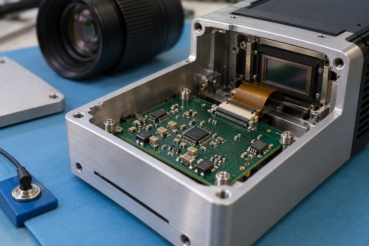
Technical details and manufacturing context for Output Amplifier
| Parameter | Typical range | Notes & selection driver |
|---|---|---|
| Supply Voltage | 3.3–5 V | Operating range for typical CCD readout ICs |
| Supply Current | 10–50 mA | Depends on output load and bandwidth |
| Bandwidth | 10–100 MHz | For high-speed CCD readout |
| Gain | 10–100 V/V | Adjustable via external resistor |
| Input Offset Voltage | ±5 mV | Max offset for accurate signal processing |
| Output Voltage Swing | 0.1–VCC-0.1 V | Rail-to-rail output for full dynamic range |
| Slew Rate | 50–500 V/µs | Ensures fast response to pixel transients |
| Input Noise Voltage Density | 5–20 nV/√Hz | Low noise for high dynamic range |
| Operating Temperature Range | -40–85 °C | Industrial grade |
| Input Capacitance | 2–10 pF | Low capacitance to minimize loading |
| Output Load Capacitance | 10–100 pF | Stable with capacitive loads |
| Package Type | SOT-23-5 | Small footprint for space-constrained designs |
Ranges are indicative industry figures for RFQ preparation, not a supplier commitment. Confirm every value and standard with the legal manufacturer before ordering.
| bandwidth: | DC to 10MHz typical, up to 100MHz for high-speed applications |
| gain range: | 20dB to 60dB programmable/adjustable |
| noise floor: | 10nV/√Hz to 100nV/√Hz input-referred noise |
| temperature: | -40°C to +85°C (industrial grade), -20°C to +70°C (commercial grade) |
| voltage range: | ±5V to ±15V supply, signal input range: ±10mV to ±2V |
Indicative industry ranges for design and RFQ preparation. Confirm the exact figures and applicable standard with the manufacturer before specifying.
Quoted from the published standard.
A practical evidence checklist for RFQ preparation and supplier evaluation.
Compare the published product scope and source details, then include your specifications and quantity in an enquiry.
Manufacturer profiles associated with Output Amplifier.
Explore company information and manufacturing capabilities, then discuss the scope of your project with a relevant supplier.
Ask for use case, specification boundaries, supplier type, and RFQ preparation information for this product.
The primary function is to receive the small charge packets from CCD pixels, convert them to voltage, and amplify them to levels suitable for further processing, while minimizing noise and maintaining signal integrity.
Typical supply voltage is 3.3–5 V, and supply current is 10–50 mA, depending on output load and bandwidth. These are reference ranges; confirm with the manufacturer for specific models.
The gain is adjustable via an external resistor, typically in the range of 10–100 V/V. The exact resistor value depends on the desired gain and must be selected according to the amplifier's specifications.
The operating temperature range is -40 to 85 °C, which is industrial grade. Ensure that the application environment stays within this range to maintain reliable operation.
This component is essential for the following industrial systems and equipment:
Editorial classification, named public sources where available, and source-reviewed manufacturer records.
Compare manufacturer profiles with relevant product and process capability.