Communication Interface ICs
View system integration details
This page explains how Clock Generator / PLL is classified within Computer, Electronic and Optical Product Manufacturing. Technical values and manufacturer relationships are research references; confirm the current specification and supplier evidence for each order.
An integrated circuit that generates and synchronizes clock signals for communication systems.
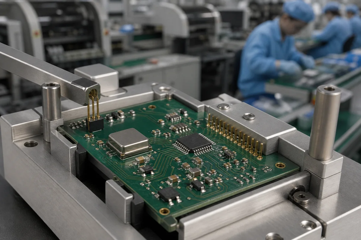
Technical details and manufacturing context for Clock Generator / PLL
| Parameter | Typical range | Notes & selection driver |
|---|---|---|
| Output Frequency Range | 1–2000 MHz | Covers common communication clock rates |
| Supply Voltage | 1.8–3.3 V | Typical for low-power ICs |
| Power Consumption | 10–500 mW | Depends on output frequency and load |
| Phase Noise | -100–-150 dBc/Hz @ 1 MHz offset | Lower is better for signal integrity |
| Jitter (RMS) | 0.1–5 ps | Critical for high-speed serial links |
| Operating Temperature Range | -40–85 °C | Industrial grade |
| Output Logic Levels | LVCMOS, LVPECL, LVDS, HCSL | Select per interface requirement |
| Frequency Stability | ±10–±100 ppm | Includes temperature and aging |
| Lock Time | 1–10 ms | Time to achieve phase lock after power-up |
| Package Type | QFN, TSSOP, BGA | Footprint and thermal performance vary |
| Number of Outputs | 1–8 | Multiple outputs for system clock distribution |
| ESD Rating | ±2000–±4000 V (HBM) | Human body modelIEC 61340-3-1 |
Ranges are indicative industry figures for RFQ preparation, not a supplier commitment. Confirm every value and standard with the legal manufacturer before ordering.
| jitter: | < 1 ps RMS (typical) |
| voltage: | 1.8V to 3.3V supply range |
| phase noise: | < -150 dBc/Hz at 1 MHz offset |
| temperature: | -40°C to +125°C (industrial grade) |
| frequency range: | 1 MHz to 2.5 GHz output |
Indicative industry ranges for design and RFQ preparation. Confirm the exact figures and applicable standard with the manufacturer before specifying.
Quoted from the published standard.
A practical evidence checklist for RFQ preparation and supplier evaluation.
Compare the published product scope and source details, then include your specifications and quantity in an enquiry.
Manufacturer profiles associated with Clock Generator / PLL.
Explore company information and manufacturing capabilities, then discuss the scope of your project with a relevant supplier.
Ask for use case, specification boundaries, supplier type, and RFQ preparation information for this product.
The directory lists a reference output frequency range of 1–2000 MHz, covering common communication clock rates. The actual range depends on the specific model and configuration; always verify with the manufacturer's datasheet.
The typical supply voltage range is 1.8–3.3 V, suitable for low-power ICs. Confirm the exact voltage requirements for your chosen part, as operation outside this range may affect performance.
The phase-locked loop continuously compares the output phase to the reference and adjusts the VCO to minimize phase error. This feedback mechanism reduces jitter, with RMS jitter values as low as 0.1 ps, critical for high-speed serial links.
The device supports LVCMOS, LVPECL, LVDS, and HCSL output logic levels. Selection depends on the interface requirements of your system; consult the datasheet for compatibility and termination guidelines.
This component is essential for the following industrial systems and equipment:
Editorial classification, named public sources where available, and source-reviewed manufacturer records.
Compare manufacturer profiles with relevant product and process capability.