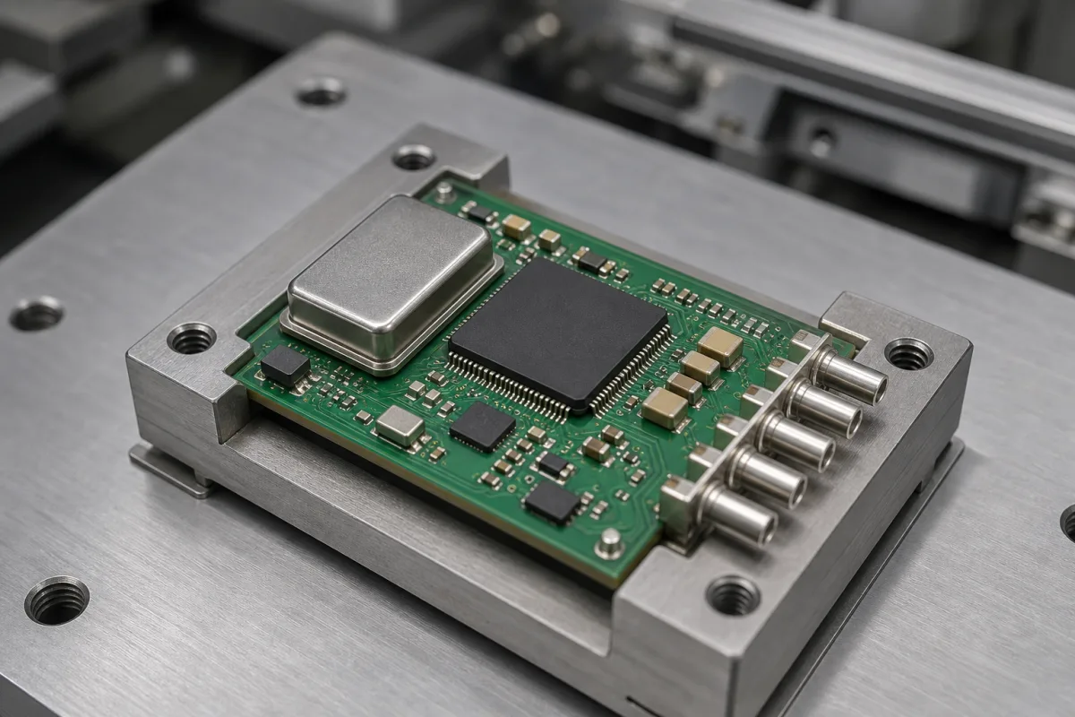
A clock generator is a chip that uses a phase-locked loop (PLL) to turn one reference, such as a crystal or input clock, into more than one output clock at the frequencies a board's processors, interfaces and converters need, as on the board pictured with a metal-can oscillator, a PLL chip and coaxial clock outputs. Ask three things first: the reference input and output frequencies, the number and signal type of outputs, and the jitter your tightest interface allows.
PLL-based clock generator and synthesizer ICs that create multiple output clocks from a crystal or reference input. Crystal oscillators themselves (see crystal oscillator), clock buffers without synthesis, real-time clocks, and network time servers and atomic clocks are outside this page.
CNFX editorial research · Sources checked October 12, 2026 · 4 sources
TI's CDCE913 is a PLL-based programmable clock synthesizer that generates up to three LVCMOS output clocks, each programmable up to 230 MHz, from a single input: an 8–32 MHz crystal or an LVCMOS clock up to 160 MHz; family members extend to four PLLs and nine outputs. Its on-chip VCXO has a ±150 ppm pull range for locking the output to an external control signal, settings are stored in EEPROM and written over a 2-wire (SDA/SCL) interface, and it runs on a 1.8 V core with 2.5–3.3 V or 1.8 V output supplies at −40 to 85 °C in a 14-pin TSSOP. [1]
TI's LMK03318 has one fractional-N PLL with integrated VCO and up to eight outputs in AC-LVPECL, AC-LVDS, AC-CML, HCSL or LVCMOS in any combination, with crystal input of 10–52 MHz or external input of 1–300 MHz, a 3.3 V core and pin, I²C or EEPROM configuration. TI says it can replace multiple oscillators and clock distribution devices. [2]
YXC's SYKG10xx clock generators list 1–333.33 MHz output, LP-HCSL, LVDS or HCSL differential pairs plus LVCMOS (from one pair to four pairs), either an internal 50 MHz crystal or an external 8–50 MHz crystal, 1.8–3.3 V supply and −40 to +85 °C. [3]
Editorial calculation: a ±150 ppm pull range on a 27 MHz reference is ±27 × 10⁶ × 150 × 10⁻⁶ ≈ ±4,050 Hz.
Give the supplier every output frequency and its signal standard (LVCMOS, LVDS, HCSL and so on), the reference (crystal frequency or input clock), jitter or phase-noise limits per output, supply rails, whether spread spectrum or frequency margining is needed, configuration method (pins, I²C, factory-programmed EEPROM), package and temperature range.
02
Set the jitter class and spread-spectrum needs
Jitter classes differ between parts by orders of magnitude, from tens of picoseconds to about 100 femtoseconds. The CDCE913 specifies cycle-to-cycle jitter of 50 ps (typ.) and 70 ps maximum and peak-to-peak period jitter of 60 ps (typ.) and 100 ps maximum, with output rise and fall times of 0.6 ns (20–80%) at 3.3 V and output duty cycle of 45–55%; TI lists it for clocks such as video, audio, USB and Ethernet, in applications such as set-top boxes and printers. [1] The LMK03318 specifies 100 fs RMS jitter (typ.) for outputs above 100 MHz and −80 dBc supply-noise rejection, and TI says its low jitter reduces bit-error rate in high-speed serial links. [2]
YXC states RMS jitter of 250–260 fs at 100 MHz and 19–98 fs against PCIe Gen5/6 limits for its SYKG10xx parts. [3] Saisi describes its AC1571 as a fully digital PLL clock generator for 5G base stations, Ethernet line cards, switches and routers, and SATA and PCI Express, with low phase noise and high supply-noise rejection. [4]
The CDCE913 also supports programmable spread-spectrum clocking (SSC) for better electromagnetic interference performance. [1] Editorial calculation: at 230 MHz the clock period is 1 ÷ 230 MHz ≈ 4.35 ns, so a 0.6 ns rise time takes about 14% of the period.
03
YXC's PCIe Gen5/6 clock generators and Saisi's AC1571
YXC lists SYKG10xx clock generators for PCIe Gen5/6 next to crystals, oscillators and clock buffers, and Saisi its AC1571 low-jitter PLL clock generator; both are described in the jitter section above. [3][4]
Ask any supplier for the datasheet with jitter or phase noise at your output frequencies and integration band, output standards and counts, reference options, supply current, SSC and margining options, programming tools and EEPROM, package, temperature range and ESD ratings.
04
Reference input, PLL and VCO, output dividers and buffers, EEPROM interface, and SSC or VCXO control
The PLL row is where the two TI parts differ: the LMK03318 uses one fractional-N PLL with integrated VCO, while the CDCE913 family extends to four PLLs and nine outputs. [2][1]
Output frequencies, reference stability, supply rails, edge rate, duty cycle, package and ESD for a clock generator order
The edge-rate, duty-cycle, storage-range and ESD figures all come from the CDCE913 datasheet; ask for the same rows for the part quoted, at your output standard.
2 companies list this product among what they make. Company figures are quoted from each
company's own website; every card states where the relationship came from.
SHENZHEN YANGXING TECHNOLOGY CO., LTD. (YXC)
Manufacturing site to be confirmed for the order
Lists SYKG10xx clock generators for PCIe Gen5/6 with crystals, oscillators and clock buffers.
Explore company information and manufacturing capabilities, then discuss the scope of your project with a relevant supplier.
Share this page
Compiled and source-reviewed by the CNFX editorial team.
Each manufacturer above links to the page on that company's own website where the product is listed, with the date we checked it. How we source and review
· Page last updated 13 October 2026
Buyer questions
How much jitter does a clock generator add?
It depends on the part: TI's CDCE913 lists 50 ps cycle-to-cycle jitter (typ.), while its LMK03318 lists 100 fs RMS (typ.) above 100 MHz. [1][2]
Can a clock generator replace more than one crystal oscillator?
TI says the LMK03318 can generate multiple clocks and replace multiple oscillators and clock distribution devices, reducing BOM cost and board area. [2]
What is spread-spectrum clocking for?
TI says the CDCE913's PLL supports spread-spectrum clocking for better electromagnetic interference performance. [1]
Sources and what still needs a direct check
Sources checked 2026-10-12. TI's CDCE913 and LMK03318 datasheets give the electrical figures; YXC's product list and Saisi's AC1571 page describe those companies' own parts.