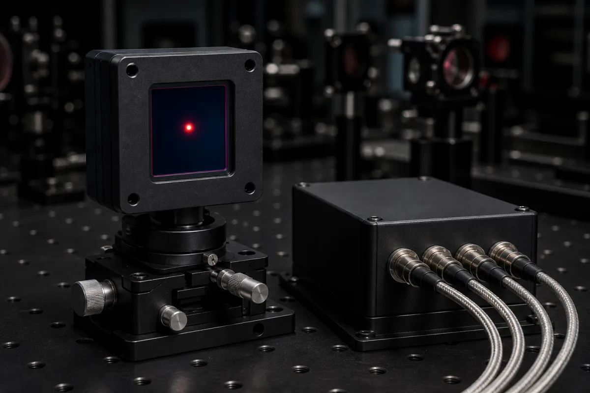
Optical position sensors · One- or two-dimensional PSD, photosensitive area, position detection error and resolution, spectral response, dark current, rise time, reverse bias, temperature and package
A position sensitive detector is a single, non-segmented silicon photodiode with a resistive surface layer: a light spot generates photocurrent that divides between electrodes in proportion to its distance from each, so the current ratio gives the spot's centre position continuously. Settle three things before choosing one: one- or two-dimensional sensing and the area the spot moves across, the position error and resolution you need, and the wavelength, speed, bias and package of your system.
One- and two-dimensional lateral-effect position sensitive detectors (PSDs) for laser displacement sensors, alignment, distance sensing, angle and vibration measurement. Segmented quadrant photodiodes, image sensors, complete laser displacement sensors and signal-processing boards sold alone are outside this page; image sensors have their own page.
CNFX editorial research · Sources checked October 12, 2026 · 4 sources
Hamamatsu's PSD technical note describes a PSD as a uniform P-type resistive layer on high-resistivity N-type silicon with output electrodes at both ends; charge generated where the light spot strikes flows to the electrodes divided in inverse proportion to distance, giving continuous position signals together with the spot's light level. It lists one-dimensional types — including visible-cut, infrared-sensitive and long types over 20 mm — and two-dimensional types, for laser displacement meters, distance sensors, optical switches and measurement of position, angle, distortion and vibration. [2]
Its S5990 and S5991 two-dimensional PSDs have photosensitive areas of 4 × 4 mm and 9 × 9 mm, with the spot position calculated from the four electrode currents over resistance lengths of 4.5 mm and 10 mm. [1]
A second maker's one-dimensional range shows the duo-lateral alternative, which places separate resistive layers on the top and bottom of the chip. OSI Optoelectronics states position accuracies of 99% over 64% of the sensing area and recommends reverse bias for current linearity at high light levels. Its SL series runs from SL3-1 (3 × 1 mm, 3 µm position detector error, 15 kΩ minimum inter-electrode resistance, 3 pF, 0.04 µs rise time) through SL15 (15 × 1 mm, 15 µm, 60 kΩ, 15 pF, 0.60 µs) and SL30 (30 × 4 mm, 30 µm, 40 kΩ, 125 pF, 1.00 µs) to SL76-1 (76 × 2.5 mm, 76 µm, 120 kΩ, 190 pF, 14.00 µs), all at 0.4 A/W responsivity. [3]
Editorial calculation: across that range the stated position detector error is about 0.1% of the active length (3 µm on 3 mm, 76 µm on 76 mm), while rise time grows from 0.04 to 14 µs as area and capacitance increase, so a longer sensor trades speed for range. Compare makers' figures only at the same spot size, wavelength and area of the sensor used. [3][1]
Give the supplier the one- or two-dimensional type, active area, position detection error and resolution required (with spot size and measurement area), wavelength, light level, reverse bias, rise time or bandwidth, dark current, temperature range, package (surface-mount, metal or ceramic), and whether a signal-processing circuit is needed, with quantity.
02
Check position error, resolution, spectral response and speed
The S5990 lists, at 25 °C: spectral response 320–1100 nm, peak sensitivity at 960 nm with 0.6 A/W, position detection error ±70 µm (typ.), ±150 µm max, at 900 nm with a 0.2 mm spot, position resolution 0.7 µm at 1 µA and 1 kHz bandwidth, dark current 0.5 nA (typ.) at 5 V, rise time 1 µs, interelectrode resistance 5–15 kΩ and 70 pF terminal capacitance. [1] The S5991 lists ±150 µm error, 1.5 µm resolution, 2 µs rise time and 500 pF. Both take 20 V maximum reverse voltage and work from −20 to +60 °C (storage −20 to +80 °C) in a ceramic surface-mount package with silicone-resin window. Errors are specified within a circle covering 80% of the area. [1]
Hamamatsu's note defines position resolution as the minimum detectable spot movement, set by noise in the output current — shot noise from the photocurrent and dark current, thermal noise from the interelectrode resistance, and op-amp noise in the current-to-voltage stage. [2]
Editorial calculation: on the S5990 the 0.7 µm resolution is 100 times finer than the ±70 µm (typ.) position detection error, so a PSD tracks small movements far better than it reports absolute position; calibrate the detector against a reference if your application needs absolute accuracy near the resolution figure. [1]
A 2025 Micromachines paper shows a large-area 2-D PSD in use: a benchmark platform for MEMS scanning mirrors built on an On-Trak PSM2-45 with a 45 × 45 mm sensing area, 1.25 µm resolution and, per its specification, 0.3% linearity. With the PSD 100 mm from the mirror, the authors calculate a measurable mechanical deflection range of −6.34° to +6.34°, and a measurement accuracy of 0.00097° at a 0.01° deflection and 0.011° at 6.34°, after accounting for optical alignment and PSD measurement error. Editorial calculation: 0.3% of the 45 mm span is 135 µm, over 100 times the 1.25 µm resolution, which is why the authors calibrated the PSD's nonlinearity before measuring. [4]
03
Error and resolution test conditions to ask every PSD supplier for
Ask each supplier for position detection error and resolution with their test spot size, wavelength, light level and bandwidth, as these figures depend on all four. [1][2]
04
Resistive layer, silicon junction, electrodes, package and signal-processing circuit
Resolution is set as much by the signal-processing circuit as by the chip: Hamamatsu traces it to shot noise, the interelectrode resistance's thermal noise and op-amp noise in the current-to-voltage stage. [2]
Part
What it controls
Fix in the order
P-type resistive layer
Position linearity; resistance; one or two layers (duo-lateral). [2][1][3]
Active area, position error, resolution, spectral range, dark current and rise time for a PSD order
The rows mix three makers' parts, Hamamatsu's 2-D S5990/S5991, OSI's 1-D duo-lateral range and a 45 × 45 mm On-Trak PSD, so compare error and resolution only at the same spot size, wavelength and area; IP rating and weight are not stated. [1][3][4]
Field
What it means and published values
Ask the supplier for
Active Area
4 × 4 mm; 9 × 9 mm (2-D); 3 × 1 to 76 × 2.5 mm (1-D duo-lateral). [1][3] 45 × 45 mm (large-area 2-D). [4]
mm.
Position Resolution
0.7 µm; 1.5 µm at 1 µA, 1 kHz. [1] 1.25 µm on a 45 × 45 mm 2-D part. [4]
Explore company information and manufacturing capabilities, then discuss the scope of your project with a relevant supplier.
Share this page
Compiled and source-reviewed by the CNFX editorial team.
Each manufacturer above links to the page on that company's own website where the product is listed, with the date we checked it. How we source and review
· Page last updated 13 October 2026
Buyer questions
How does a position sensitive detector work?
Photocurrent from the light spot divides through a resistive layer between electrodes in inverse proportion to distance, so the current ratio gives the spot position. [2]
How accurate is a PSD?
Hamamatsu's 4 × 4 mm S5990 lists ±70 µm (typ.) position detection error and 0.7 µm resolution. [1]
What wavelengths can a silicon PSD detect?
The S5990 responds from 320 to 1100 nm, peaking at 960 nm. [1]
Where are PSDs used?
In laser displacement meters, distance sensors, optical switches and measurement of position, angle, distortion and vibration. [2]
How does a duo-lateral PSD differ from a single-layer one?
It has separate resistive layers on the top and bottom of the chip; one maker states 99% position accuracy over 64% of the sensing area for its one-dimensional range. [3]
How accurately can a 2-D PSD measure a scanning mirror's angle?
A 2025 Micromachines study using a 45 × 45 mm On-Trak PSM2-45 PSD (1.25 µm resolution, 0.3% linearity) 100 mm from a MEMS mirror calculated a ±6.34° range, with accuracy of 0.00097° at 0.01° deflection and 0.011° at 6.34°. [4]
Sources and what still needs a direct check
Sources checked 2026-10-12. Hamamatsu's S5990/S5991 datasheet and PSD technical note are used to show what a PSD specification covers, with OSI Optoelectronics' duo-lateral range as a second maker's example and a 2025 Micromachines paper as an application study; values for your order must come from the supplier's datasheet.