Detector Array
View system integration details
This page explains how Readout Circuit is classified within Computer, Electronic and Optical Product Manufacturing. Technical values and manufacturer relationships are research references; confirm the current specification and supplier evidence for each order.
Electronic circuit that processes and converts signals from detector elements into usable data.
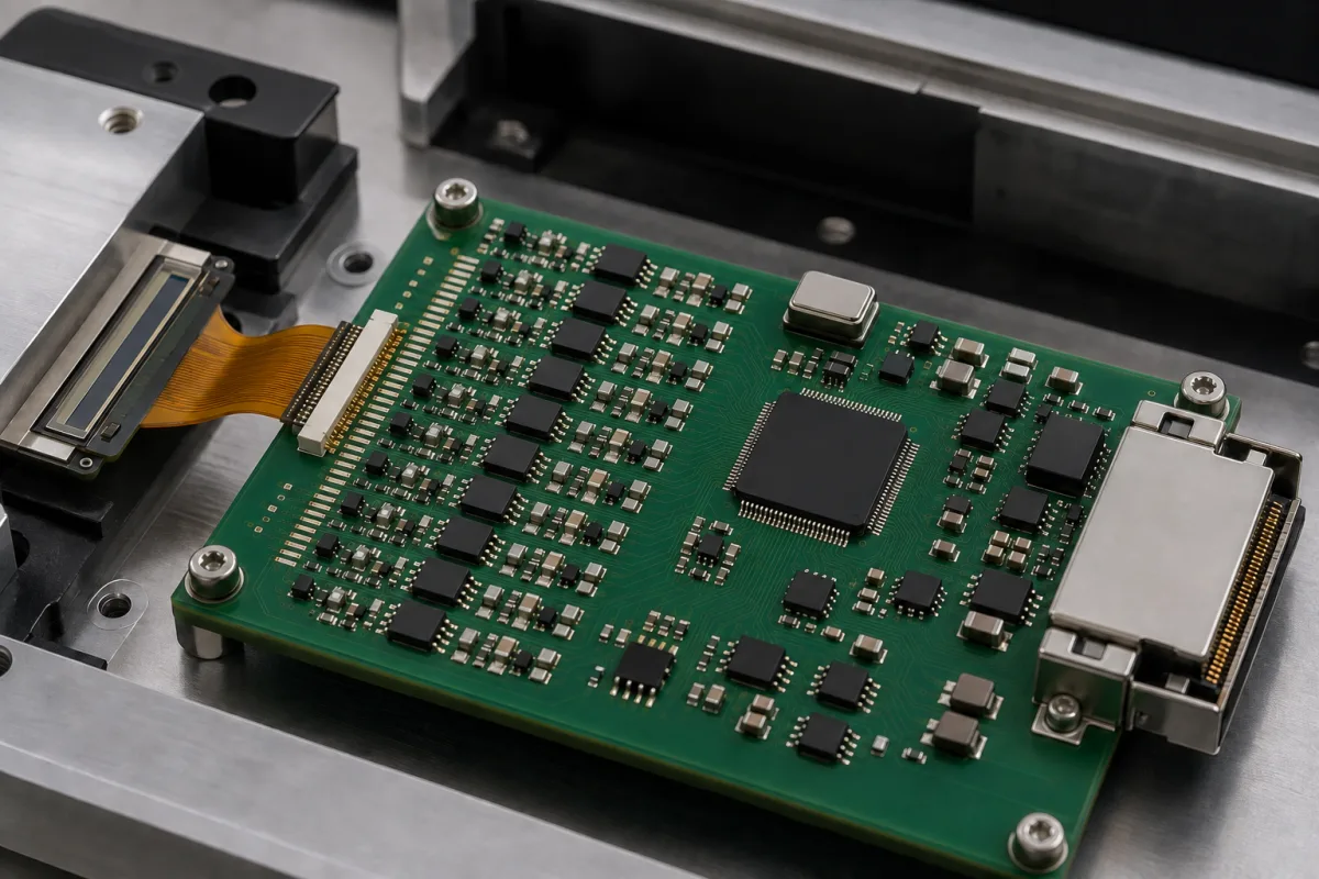
Technical details and manufacturing context for Readout Circuit
| Parameter | Typical range | Notes & selection driver |
|---|---|---|
| Supply Voltage | 3.3–5 V | Typical CMOS logic levels |
| Power Consumption | 50–200 mW | Depends on pixel array size and frame rate |
| Input Referred Noise | 10–50 e- rms | Lower is better for low-light imaging |
| Conversion Gain | 10–100 µV/e- | Higher gain improves sensitivity |
| Pixel Rate | 10–100 MHz | Determines maximum frame rate |
| ADC Resolution | 12–16 bit | Higher resolution for better dynamic range |
| Operating Temperature | -40–85 °C | Industrial grade |
| Storage Temperature | -55–125 °C | Non-operating |
| Relative Humidity | 5–95 % | Non-condensing |
| ESD Tolerance | 2–4 kV HBM | Human body modelIEC 61340-3-1 |
| Package Type | CLCC-48–CLCC-84 pin | Ceramic package for hermeticity |
| Weight | 1.5–5.0 g | Depends on package size |
Ranges are indicative industry figures for RFQ preparation, not a supplier commitment. Confirm every value and standard with the legal manufacturer before ordering.
| pressure: | Atmospheric (non-pressurized) |
| other spec: | Signal frequency range: DC to 10 MHz, Power supply: 3.3V to 5V DC |
| temperature: | -40°C to +85°C |
Indicative industry ranges for design and RFQ preparation. Confirm the exact figures and applicable standard with the manufacturer before specifying.
Quoted from the published standard.
A practical evidence checklist for RFQ preparation and supplier evaluation.
Compare the published product scope and source details, then include your specifications and quantity in an enquiry.
Manufacturer profiles associated with Readout Circuit.
Explore company information and manufacturing capabilities, then discuss the scope of your project with a relevant supplier.
Ask for use case, specification boundaries, supplier type, and RFQ preparation information for this product.
It processes and converts analog signals from detector elements into digital data for analysis.
Supply voltage is typically 3.3–5 V, and power consumption ranges from 50–200 mW, depending on array size and frame rate.
Input referred noise is given in electrons RMS, typically 10–50 e- rms, with lower values preferred for low-light imaging.
ESD tolerance is specified per IEC 61340-3-1, with typical values of 2–4 kV HBM. Verify compliance with the manufacturer.
This component is essential for the following industrial systems and equipment:
Editorial classification, named public sources where available, and source-reviewed manufacturer records.
Compare manufacturer profiles with relevant product and process capability.