Editorial Technical Reference

Amplification Stage

This page explains how Amplification Stage is classified within Computer, Electronic and Optical Product Manufacturing. Technical values and manufacturer relationships are research references; confirm the current specification and supplier evidence for each order.

Technical Definition & Core Assembly

Electronic circuit stage that increases the amplitude of input signals while maintaining signal integrity.
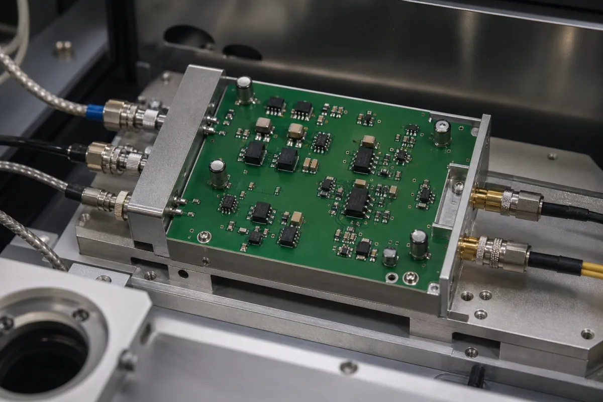
Representative product image. Confirm appearance and specifications with the manufacturer.

Product Specifications

Technical details and manufacturing context for Amplification Stage

Definition
The Amplification Stage is a component used in signal processing systems within the computer, electronic, and optical product manufacturing industry. Its primary function is to increase the amplitude of weak input signals to usable levels while preserving signal integrity. This stage typically follows initial signal conditioning and precedes further processing or output stages. It is designed to minimize noise, distortion, and interference during amplification. The stage utilizes active electronic components such as transistors or operational amplifiers configured in specific topologies like common-emitter, common-source, or differential pairs to provide voltage, current, or power gain. Feedback networks may be employed to control gain, bandwidth, and stability. Key parameters include adjustable gain (20–40 dB), bandwidth (10–100 MHz at -3 dB point), input voltage range (±5 V), output voltage swing (±10 V into 10 kΩ load), dual supply voltage (±12–±15 V DC), input impedance (1–10 MΩ), output impedance (50–100 Ω), total harmonic distortion (≤0.01% at 1 kHz, 1 Vrms output), noise figure (≤3 dB at 50 Ω source impedance), operating temperature (-40–85 °C), humidity (5–95% RH non-condensing), dimensions (25×20×10 mm), and weight (approximately 15 g). The stage is typically a PCB mount module. Materials on file include semiconductor silicon, copper, FR-4 substrate, and solder alloy. No specific standards are listed. For procurement, verify model-specific values and standards with the legal manufacturer or supplier. The stage is intended for industrial applications where signal amplification is required. It is not a complete amplifier system but a component stage. Proper operation requires appropriate power supply and signal conditioning. Failure boundaries include exceeding input voltage range, which may cause clipping or damage. Maintenance signals include degraded signal quality or increased distortion. Selection inputs include required gain, bandwidth, and impedance matching. Interfaces include input and output connections, power supply pins, and possibly feedback network connections. Verification questions should address gain accuracy, bandwidth, distortion, and noise performance under specified conditions.
Working Principle
The amplification stage operates by using active components like transistors or operational amplifiers in configurations such as common-emitter, common-source, or differential pairs. These components are biased to operate in their active regions, allowing them to control a larger output signal based on a smaller input signal. The gain is determined by the circuit topology and component values. Feedback networks may be used to set precise gain, improve linearity, and control bandwidth. The stage provides voltage, current, or power gain depending on the configuration. Input impedance is high to minimize loading of the source, while output impedance is low to drive subsequent stages or cables. The power supply provides the necessary energy for amplification. The stage is designed to operate within specified voltage and temperature ranges to maintain performance.
Common Materials
Semiconductor silicon, Copper, FR-4 substrate, Solder alloy
Technical Parameters
ParameterTypical rangeNotes & selection driver
Gain20–40 dBAdjustable; higher gain may reduce bandwidth.
Bandwidth10–100 MHzAt -3 dB point; depends on gain setting.
Input Voltage Range±5 VExceeding may cause clipping or damage.
Output Voltage Swing±10 VInto 10 kΩ load.
Supply Voltage±12–±15 V DCDual supply required.
Input Impedance1–10 High impedance minimizes loading.
Output Impedance50–100 ΩLow output for driving cables.
Total Harmonic Distortion≤0.01 %At 1 kHz, 1 Vrms output.
Noise Figure≤3 dBAt 50 Ω source impedance.
Operating Temperature-40–85 °CIndustrial grade.
Humidity5–95 % RHNon-condensing.
Dimensions25×20×10 mmPCB mount module.
Weight15 gApproximate.

Ranges are indicative industry figures for RFQ preparation, not a supplier commitment. Confirm every value and standard with the legal manufacturer before ordering.

Components / BOM
  • Active Device
    Provides amplification through controlled electron flow (transistor, op-amp)
    Material: Semiconductor (silicon, gallium arsenide)
  • Bias Network Part
    Establishes proper operating point for active device
    Material: Resistors, capacitors, diodes
  • Input Coupling Part
    Connects input signal to amplification circuit while blocking DC
    Material: Capacitors, transformers
  • Output Coupling Part
    Connects amplified signal to next stage while blocking DC
    Material: Capacitors, transformers
  • Feedback Network Optional Part
    Controls gain, bandwidth, and stability characteristics
    Material: Resistors, capacitors

Applied To / Applications

This component is essential for the following industrial systems and equipment:

Industrial Ecosystem & Supply Chain Structure

Complementary Systems
Downstream Applications
Specialized Tooling

Application Fit & Sizing Matrix

Operational Limits
pressure: Atmospheric to 1.5 bar (sealed enclosure dependent)
other spec: Input signal range: ±10V max, Output current: 20mA max, Power supply: ±15VDC, Bandwidth: DC to 100kHz
temperature: -40°C to +85°C (operational), -55°C to +125°C (storage)
Media Compatibility
✓ Low-voltage analog signals ✓ Sensor output conditioning ✓ Audio frequency processing
Unsuitable: High-voltage power switching environments (>100V)
Sizing Data Required
  • Input signal amplitude range
  • Required gain (V/V or dB)
  • Load impedance (Ω)

Reliability & Engineering Risk Analysis

Failure Mode & Root Cause
Cavitation
Cause: Localized pressure drops below vapor pressure, forming and collapsing vapor bubbles that cause surface pitting and material fatigue, often due to improper fluid velocity, temperature, or suction conditions.
Abrasive erosion
Cause: High-velocity particulate matter in the fluid stream impacting internal surfaces, leading to gradual material loss and dimensional changes, typically from inadequate filtration or contaminated process media.
Maintenance Indicators
  • Unusual high-frequency vibration or audible knocking sounds indicating cavitation or impeller imbalance
  • Progressive drop in output pressure or flow rate despite constant input, signaling internal wear or blockage
Engineering Tips
  • Implement real-time pressure and temperature monitoring with automated controls to maintain operating parameters within optimal ranges, preventing cavitation conditions
  • Install multi-stage filtration systems with regular maintenance schedules to remove particulates, and apply wear-resistant coatings or materials on high-velocity contact surfaces

Indicative industry ranges for design and RFQ preparation. Confirm the exact figures and applicable standard with the manufacturer before specifying.

Compliance & Manufacturing Standards

Applicable Standards
ANSI/ISA-95.00.01-2010 - Enterprise-control system integration DIN EN 61000-6-2:2019 - Electromagnetic compatibility

Quoted from the published standard.

Manufacturing Precision
  • Gain accuracy: +/-0.5 dB
  • Frequency response flatness: +/-0.1 dB
Quality Inspection
  • Harmonic distortion measurement
  • Signal-to-noise ratio verification

Manufacturers of Amplification Stage

Manufacturer profiles associated with Amplification Stage.

Sourcing Amplification Stage from China?
Tell us your specification and target quantity — we will match it against manufacturer records and come back with the factories that fit.
Request manufacturers We manufacture this

Manufacturer listings support early research and capability understanding. They are not certification, ranking, or transaction guarantees.

Technical documentation
Request current drawings, revision history, and a signed specification sheet.
Manufacturing capability
Verify equipment lists, process limits, capacity, and representative production evidence.
Inspection readiness
Confirm test methods, calibrated equipment, sampling plans, and traceable reports.
Supplier transparency
Check the legal entity, factory address, ownership, certifications, and direct contacts.

CNFX does not score or rank suppliers. Buyers must verify all claims and documents with the legal manufacturer before ordering.

Supply Chain Compatible Machinery & Devices

Modular Industrial Edge Computing Device

This modular industrial edge computing device is a ruggedized system designed for deployment in harsh industrial environments to perform real-time data processing, analytics, and control functions at the network edge.

Explore Specs →
Industrial Smart Camera Module

The Industrial Smart Camera Module is a compact, self-contained vision processing unit designed for integration into industrial machinery and production lines.

Explore Specs →
Surface Mount Resistor

Passive electronic component for current limiting and voltage division in circuits

Explore Specs →
Surface Mount Capacitor

A surface mount capacitor is a fundamental electronic component used for energy storage, filtering, coupling, and decoupling in electronic circuits.

Explore Specs →

Frequently Asked Questions

What is the typical gain range of this amplification stage?

The gain is adjustable and typically ranges from 20 to 40 dB. However, higher gain may reduce bandwidth. Verify the exact gain range for your specific model with the manufacturer.

What power supply is required?

The stage requires a dual DC supply voltage of ±12 to ±15 V. Ensure the power supply is within this range and can provide adequate current.

What is the input impedance and why is it important?

The input impedance is 1 to 10 MΩ. High input impedance minimizes loading of the signal source, preserving signal integrity. Verify the exact value for your application.

What are the operating temperature limits?

The operating temperature range is -40 to 85 °C, industrial grade. Ensure the environment stays within this range to avoid performance degradation or damage.

Data Basis

Editorial classification, named public sources where available, and source-reviewed manufacturer records.

Preliminary Technical Classification
This page supports structured research, RFQ preparation, and supplier evaluation. It does not replace buyer-led supplier qualification, standards review, or technical approval.
Buyer enquiry

Request manufacturing insight for Amplification Stage

Ask for use case, specification boundaries, supplier type, and RFQ preparation information for this product.

Where it goes
Straight to the CNFX editorial desk, and to the manufacturer if this product is linked to a claimed profile. Nothing is broadcast to a supplier list.
Your details stay here
We do not sell or rent enquiry data, and we do not add you to a mailing list. Used only to answer this request.
No commission, no middleman
CNFX is a directory. We take no cut of any order and never negotiate on a supplier's behalf.
What we don't claim
A listing is not an endorsement. Qualify every supplier and verify every figure yourself before ordering.

Your business information is used only to process this request.

Thank you! Your message has been sent. We'll respond within 1–3 business days.
Sorry, we couldn't send your message. Please try again, or email us at contact@cnfx.com.

Need to Manufacture Amplification Stage?

Compare manufacturer profiles with relevant product and process capability.

Previous Product
XY Positioning Stage
Last Product
Get QuotesChat