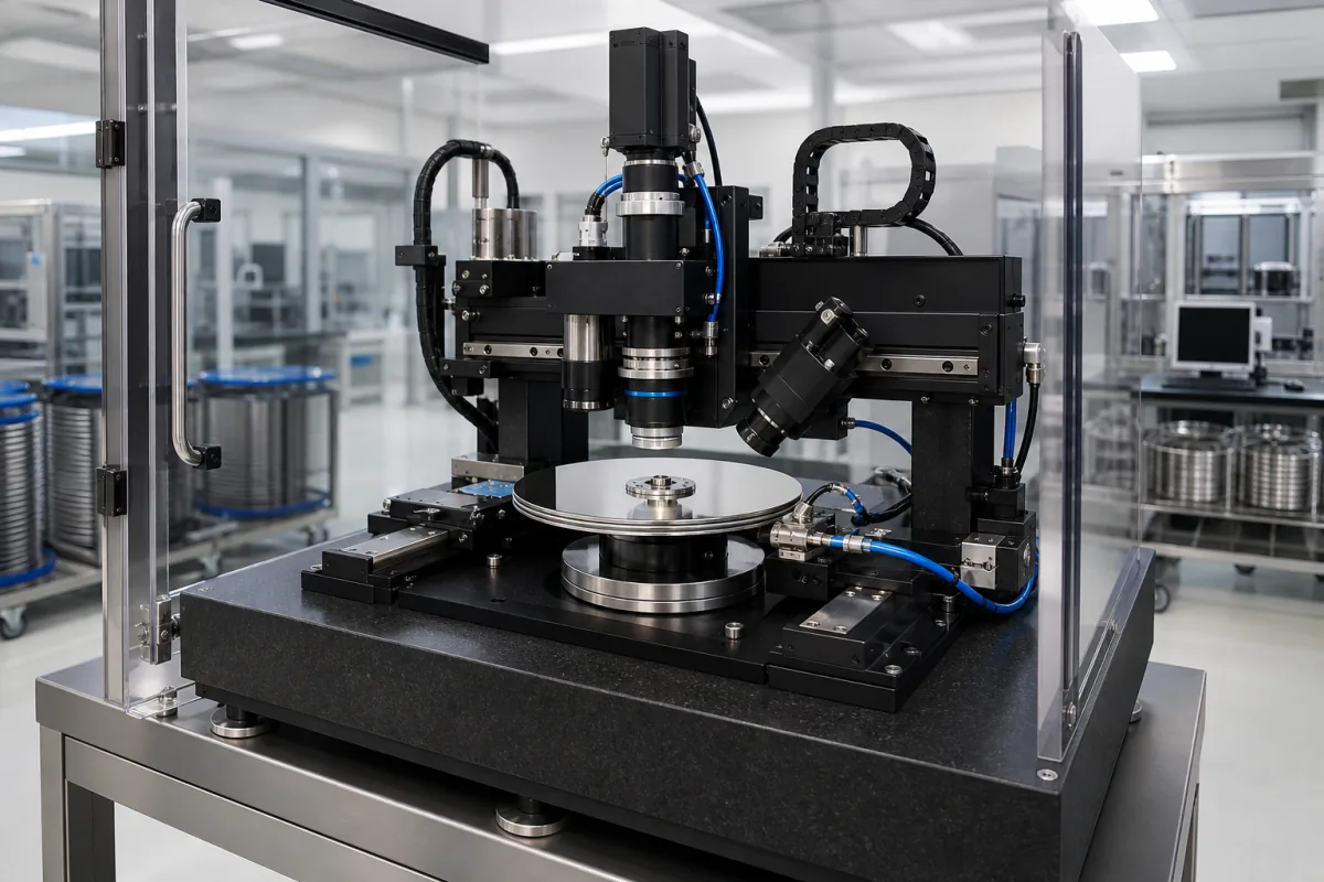
Optical surface analyzer for spinning disks and wafers: laser slope, phase and scatter channels that map and classify scratches, particles, pits and stains
Inspection of polished disks and wafers spun under a laser · slope and phase channels for topography and films, a scatter channel for particles and scratches, and the defect classes the report sorts them into
A hard-disk platter or a polished wafer can fail for a scratch a few tens of nanometres deep, a particle, a stain that changes the film but not the height, or a pit. An optical surface analyzer finds them by spinning the part on a precision spindle while a focused laser spot walks across the radius, so the whole face is covered in a spiral. Separate detectors read the same spot at once: position-sensitive detectors measure the slope of the surface, a polarisation channel measures the phase shift that thin films and stains cause, and a scatter detector picks up light thrown sideways by particles and scratches. Software combines the channels into a defect map and sorts each event into a class.
Laser-scanning optical surface analyzers for polished, rotating substrates: hard-disk platters and glass or NiP-plated substrates, silicon, silicon carbide and other wafers, with slope (profilometer), phase-shift (ellipsometric), reflectivity and scatter channels and automatic defect classification. Lens form, centration and wavefront measurement are covered on the Precision optical lens inspection and measurement system page; interferometric probe heads for distance and thickness are covered on the Interferometric optical head page. Patterned-wafer inspection, coordinate measuring machines and AFM are outside this page.
CNFX editorial research · Sources checked October 13, 2026 · 3 sources
Two oblique lasers, quadrant detectors and a scatter photodiode: how one spot gives slope, phase and scatter at once
Candela Instruments' European patent EP 1 245 922 describes the optical layout behind this class of instrument. Its point is that topographic defects (scratches, pits, mounds, particles) and non-topographic ones (stains, inclusions) need different channels, and that one scan can carry all of them.
The patent states that the miniaturised designs it describes can measure sub-micron scratches, particles, stains, pits, mounds, handling damage, wear of the carbon layer, outside-diameter damage and contamination, and the longitudinal Kerr effect. [1] On a finished disk the layers being inspected are thin: Candela gives 20 to 200 Å of carbon overcoat (typ.) and 10 to 30 Å of fluorocarbon lubricant (typ.), on a substrate of NiP-plated Al-Mg alloy or glass (typ.). [1]
Editorial calculation: from the patent's sin θ / cos² θ factor, height sensitivity at 60° is about 3.5 (0.866 ÷ 0.25) against about 1.4 at 45° (0.707 ÷ 0.5), roughly 2.4 times higher. Assuming a 95 mm platter, one pulse of a 1,024-pulse encoder spans about 0.29 mm of the outer circumference (π × 95 ÷ 1,024); the patent multiplies the encoder signal with a phase-locked loop by a selectable factor to get a finer position, and says this lets repeated revolutions be averaged without losing lateral resolution. [1]
Element in the patent
Value or arrangement
What it measures
Light sources
Laser diodes at 780 or 655 nm, P, S or 45° polarised [1]
Illuminate one spot on the disk or wafer
Angle of incidence
Any angle except normal; about 60° in the preferred embodiment, with height sensitivity rising as sin θ / cos² θ [1]
Larger angles also raise the signal from transparent substrates [1]
Two beams at right angles
Second laser and detector rotated 90° from the first [1]
Radial and circumferential slope separated from height [1]
Quarter-wave plate, polarising splitter at 45°, two quadrant detectors
Split the reflected beam into polarisation components [1]
Phase shift: films, stains and other non-topographic defects [1]
Give the substrate (glass, NiP/Al, Si, SiC; diameter and thickness), whether it is transparent, the films on it, and which defect types must be separated; ask for the laser wavelengths, angle of incidence and the channels the instrument records.
02
Defect classes a production report uses: 11 categories on a SiC substrate, from scratch and particle to IDL and bump
What the buyer receives is a classified defect map. A 2025 study from National Yang Ming Chiao Tung University and partners inspected 150 mm 4H-SiC substrates and epi-wafers on a KLA Candela 8520 in a Class 10 mini-environment, and its tables show the classes and counts such a report carries.
After epitaxy the same tool reported a different class list, including shallow triangles, pit triangles, basal plane dislocations (BPD), carrots, BSF and SSF; the 12 µm epi-wafer showed 170 defects in total and 56 SSF. [2] Scratches the analyzer flagged on the substrate were cut by focused ion beam and measured by SEM at 99.29 nm and 136.9 nm deep, and the authors found that scratches of around 100 nm depth did not transfer into the epitaxial layer. [2] They also note that industrial specifications permit a finite level of scratches on SiC substrates depending on wafer diameter, giving cumulative scratch lengths of 50 mm or less in 200 mm production as an example. [2]
Editorial calculation: small particles make up 130 of the 139 events on the 12 µm substrate scan, about 94 %, so the class definitions and size thresholds set in the recipe govern that 94 % share of the count. [2]
Ask which defect classes the recipe reports, the size threshold of each, how scratches are measured (count, length or both), and whether the defect map exports to SEM or FIB review.
03
Defects below the surface that an optical surface analyzer does not resolve: threading dislocations in SiC
The scan reads the surface and the light it returns. A researcher choosing an analyzer for substrate grading should know where that stops.
A 2025 study from Chung Yuan Christian University and LEAP Semiconductor states that commercial surface inspection tools such as KLA Candela and Lasertec SICA, which combine optical inspection with photoluminescence channels, are used for extended defects in SiC epilayers such as stacking faults and surface topographic defects, but are ineffective for threading dislocations, which have weak or no optically detectable surface features. [3] The authors' confocal subsurface defect-PL method reaches a spatial resolution of about 1.3 µm, set by optical diffraction, against about 16 µm and an imaging contrast of about 0.4 reported for an earlier PL-quenching method. [3]
Editorial calculation: 16 µm against 1.3 µm is roughly a twelvefold difference in resolution (16 ÷ 1.3), which is why threading-dislocation grading of SiC substrates is bought as a separate PL or X-ray measurement rather than as a surface-analyzer recipe. [3]
If dislocations or other subsurface defects must be graded, specify that separately; do not expect the surface scan to report them.
04
Details for an optical surface analyzer enquiry
Paste it into your enquiry below or into an email to a maker, then replace every bracket.
Substrates: [glass or NiP/Al disk; Si; SiC; diameter; thickness; transparent or not]
Films on the surface: [carbon, lubricant, oxide; thickness]
Defects to classify: [scratch, particle, pit, stain, mound, others; size thresholds]
Channels needed: [scatter; slope/topography; phase or ellipsometric; PL]
Throughput and handling: [manual or automatic loading; parts per hour]
Environment: [cleanroom class; mini-environment]
Output: [defect map format; SEM/FIB coordinate export]
Explore company information and manufacturing capabilities, then discuss the scope of your project with a relevant supplier.
Share this page
Compiled and source-reviewed by the CNFX editorial team.
Each manufacturer above links to the page on that company's own website where the product is listed, with the date we checked it. How we source and review
· Page last updated 13 October 2026
Buyer questions
What does an optical surface analyzer measure on a hard-disk platter?
Candela's patent lists sub-micron scratches, particles, stains, pits, mounds, handling damage, carbon-layer wear, contamination and the Kerr effect, read from slope, phase and scatter channels in one scan. [1]
Why use an oblique laser angle?
Height sensitivity rises with sin θ / cos² θ; Candela prefers about 60°, which also raises the signal from transparent substrates. [1]
What defect classes appear in a SiC wafer report?
A KLA Candela 8520 scan in a 2025 study reported scratch, particle, small particle, pit, stain, macro pit, micropipe, IDL, stacking fault and bump on substrates. [2]
Can the analyzer find threading dislocations in SiC?
A 2025 study states that surface tools such as KLA Candela and Lasertec SICA are ineffective for threading dislocations because they have weak or no surface features. [3]
Sources and what still needs a direct check
Sources checked 2026-10-13. Three sources: Candela Instruments' European patent application EP 1 245 922 on combined slope, phase and scatter measurement, a 2025 Micromachines study of CMP scratches on SiC wafers inspected with a KLA Candela 8520, and a 2025 Nanoscale Advances study on detecting threading dislocations in SiC.