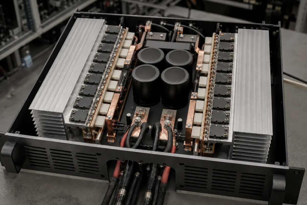
Paralleled bipolar output stage for high-power linear amplifiers: 230–260 V transistors in rows on the heat sinks
The paralleled bipolar output devices of a high-power linear amplifier · device ratings, second-breakdown limits that decide how many are needed, and gain ranks
In a large linear amplifier the output stage is the row of power transistors along each heat sink: NPN devices on one rail, PNP devices on the other, all doing the same job in parallel so that no single device has to carry the full load current at the full voltage across it. How many devices a stage needs has to be checked against their safe operating area at the voltage they see, not only against their headline power rating. This page compares three published device families on those points.
Discrete bipolar output stages of high-power linear (class AB and similar) audio and professional amplifiers: the paralleled complementary output transistors, their safe operating area and gain matching. Solid-state RF and microwave output amplifiers are covered on the RF output stage amplifier page; amplifier boards built on monolithic power ICs are covered on the Linear (class AB) amplifier module page; integrated DrMOS-type smart power stages for DC-DC converters are outside this page.
CNFX editorial research · Sources checked October 12, 2026 · 3 sources
230–260 V, 15–17 A and 150–200 W per device: three output transistors compared
Toshiba describes its 2SC5200 NPN transistor, complementary to the 2SA1943, as suited to the output stage of a 100 W high-fidelity audio amplifier. [1] onsemi lists its MJL3281A (NPN) and MJL1302A (PNP) for professional audio amplifiers, theatre and stadium sound systems and public address systems. [2] Sanken lists the 2SC3264, complementary to the 2SA1295, for audio and general purpose. [3]
onsemi gives a junction-to-case thermal resistance of 0.625 °C/W and a derating of 1.43 W/°C above 25 °C for the MJL3281A; all three devices are rated for a 150 °C junction. [2][1][3] Editorial calculation: at 0.625 °C/W, holding the junction at 150 °C with the case at 75 °C allows (150 − 75) / 0.625 = 120 W per device, before case-to-sink and sink resistance are added.
The 150–200 W ratings apply with the case held at 25 °C; dissipation per device in a real stage is set by case temperature and by the safe operating area below.
02
Second breakdown: 4 A at 50 V but only 1 A at 100 V per device, which sets the device count
onsemi names two limits on a transistor's power handling, average junction temperature and second breakdown, and bases its safe-operating-area curves on a 150 °C peak junction, noting that at high case temperatures the thermal limit reduces power below the second-breakdown limit. [2] For the MJL3281A/MJL1302A it specifies a second-breakdown collector current, base forward biased, of 4 A at VCE = 50 V and 1 A at VCE = 100 V, for 1 s non-repetitive. [2]
Editorial calculation: doubling the voltage across the device from 50 V to 100 V cuts the allowed current by four and the allowed power by half, so where a design's worst case puts a high voltage across a conducting device, the number of devices in parallel follows from this limit rather than from the dissipation rating alone. The 10 A load current in the table is an illustrative figure, not a value from the sources.
Voltage across the conducting device
Second-breakdown current per device (1 s)
Editorial calculation: power per device
Editorial calculation: devices to carry 10 A at that voltage
Ask for the stage's worst-case voltage and current per device, with the device count and the safe-operating-area curve used to justify it.
03
Gain ranks and NPN/PNP matching for devices that share current
Paralleled devices are bought by gain rank. Toshiba sorts the 2SC5200 into rank R (hFE 55–110) and rank O (80–160) at VCE = 5 V, IC = 1 A. [1] Sanken ranks the 2SC3264 as O (50–100) and Y (70–140) at VCE = 4 V, IC = 5 A. [3] onsemi specifies hFE of 75 to 150 for the MJL3281A from 0.5 A to 5 A (45 minimum at 8 A) and NPN/PNP gain matching within 10% from 50 mA to 5 A. [2]
Editorial calculation: within a single Toshiba or Sanken rank the highest permitted gain is twice the lowest (110 / 55, 160 / 80, 100 / 50, 140 / 70), so the rank alone does not make two devices alike; a purchase specification can name a rank, a narrower matched tolerance, or the maker's complementary matching.
04
Data for an amplifier output stage enquiry
Paste it into your enquiry below or into an email to a maker, then replace every bracket.
Amplifier: [output power per channel; load impedance and minimum; rail voltages]
Devices: [type and maker; package; number of NPN/PNP per channel]
Safe operating area: [worst-case VCE and IC per device; time; case temperature]
Matching: [hFE rank; matched sets; NPN/PNP complementary matching]
Thermal: [heat sink; case-to-sink insulation; fan]
Explore company information and manufacturing capabilities, then discuss the scope of your project with a relevant supplier.
Share this page
Compiled and source-reviewed by the CNFX editorial team.
Each manufacturer above links to the page on that company's own website where the product is listed, with the date we checked it. How we source and review
· Page last updated 13 October 2026
Buyer questions
Why does a high-power amplifier put output transistors in parallel?
Because each device's safe current falls steeply with voltage: onsemi's MJL3281A allows 4 A at 50 V but only 1 A at 100 V for 1 s, so high-rail stages spread the current over more devices. [2]
What power does Toshiba suggest for one 2SC5200/2SA1943 pair?
Toshiba describes the pair as suited to the output stage of a 100 W high-fidelity audio amplifier. [1]
How much heat can one MJL3281A dissipate?
200 W with the case at 25 °C; editorial calculation from its 0.625 °C/W gives 120 W with the case at 75 °C. [2]
How are output devices matched?
By gain rank, such as Toshiba's R (55–110) and O (80–160); onsemi specifies NPN/PNP gain matching within 10% for the MJL3281A/MJL1302A. [1][2]
Sources and what still needs a direct check
Sources checked 2026-10-12. Device ratings, safe-operating-area limits and gain ranks come from the Toshiba 2SC5200, onsemi MJL3281A/MJL1302A and Sanken 2SC3264 data sheets. Values apply to the devices named.