Vacuum processing chamber for CsI:Tl scintillator evaporation: twin effusion cells, a heated rotating substrate holder and the pressure that sets columnar growth
The chamber in which X-ray scintillator layers are grown · effusion cells for caesium iodide and thallium iodide, a heated rotating substrate holder, and the pressure and temperature that decide whether the layer grows as light-guiding columns
A caesium iodide scintillator converts X-rays into visible light that a silicon sensor can read, and when it is grown as fine columns those columns guide the light straight down instead of letting it spread. The columns are made in a vacuum chamber: CsI and a thallium dopant are evaporated from heated cells, and the vapour condenses on a heated, rotating substrate above. The chamber's pressure, the substrate temperature, the source arrangement and the deposition rate together decide the layer's structure, its thallium content and so its brightness and sharpness.
Vacuum chambers and their in-chamber equipment used to grow thallium-doped caesium iodide (CsI:Tl) scintillator layers by thermal evaporation for X-ray imaging detectors: effusion cells or boats for CsI and thallium iodide, heated and rotating substrate holders, pressure control with inert gas, and post-deposition heat treatment. General-purpose process and test chambers, their materials, outgassing and leak testing are covered on the Vacuum chamber page; the welded chamber shell and flanges on the Vacuum chamber body page; door hinges on the Vacuum chamber door hinge system page; steel degassing tanks on the Degassing chamber for liquid steel page; and optical coating chambers on the Optical lens vacuum coating chamber page.
CNFX editorial research · Sources checked October 13, 2026 · 4 sources
Columns or a dense layer: what 10⁻² Torr, 10⁻⁵ Torr and 5·10⁻³ Pa did to CsI:Tl in three chambers
Three groups report the chamber conditions they used; the first shows the pressure itself switching the structure between columns and a dense layer.
Editorial calculation: 10⁻² Torr is about 1.3 Pa and 10⁻⁵ Torr about 1.3 × 10⁻³ Pa, so the NanoFocusRay and KAIST comparison spans three decades of pressure; BINP's 5·10⁻³ Pa (about 4 × 10⁻⁵ Torr) lies between the two. [1][3] At BINP's 17 Å/s, a layer grows about 6.1 µm per hour, so its 14 µm film needed roughly 2.3 hours; the same rate would need about 38 hours for the 230 µm screens the IHEP group tested, which shows why the deposition rate is a design figure for a production chamber. [3][4]
The chamber therefore needs a way to hold the chosen pressure during evaporation, not only to reach base pressure: the KAIST group controlled process pressure by injecting argon. [2]
State the layer thickness and structure required (columnar or dense), the substrate size and material, the base and process pressure, the substrate temperature range and the target deposition rate.
02
Separate cells for CsI and thallium iodide: 660 °C against 440 °C, and thallium that runs out above 10 µm
The dopant evaporates more readily than the host, which shapes how the sources inside the chamber are laid out.
Editorial note: when a single boat holds both materials, the thallium content falls as the run goes on (BINP's 80 % figure at 8 µm). Separate, independently heated cells, or a step-wise process, are the two answers the sources describe. [3][1]
Finding
Value
Source
Melting points
CsI 660 °C; TlI 440 °C; for a simple evaporation process the KAIST group writes that “Most of TlI particles are supposed to be evaporated before CsI powder melts”
Specify the number of sources, their maximum temperature and control, the target Tl concentration and how it will be held through the layer thickness.
03
After deposition: 250 to 400 °C heat treatment, 200 hours to even out thallium, and how thickness and substrate trade light against sharpness
What happens in or after the chamber also sets the finished screen's performance.
Editorial calculation: on graphite, tripling the thickness from 70 to 230 µm (3.3 times) raised relative light output 4.3 times, while on fibre optic plate the same change raised it about 1.9 times (8.7 ÷ 4.6). [4] Substrate and thickness are therefore part of the chamber specification, because the holder has to carry the chosen substrate at the chosen temperature for the hours a thick layer takes.
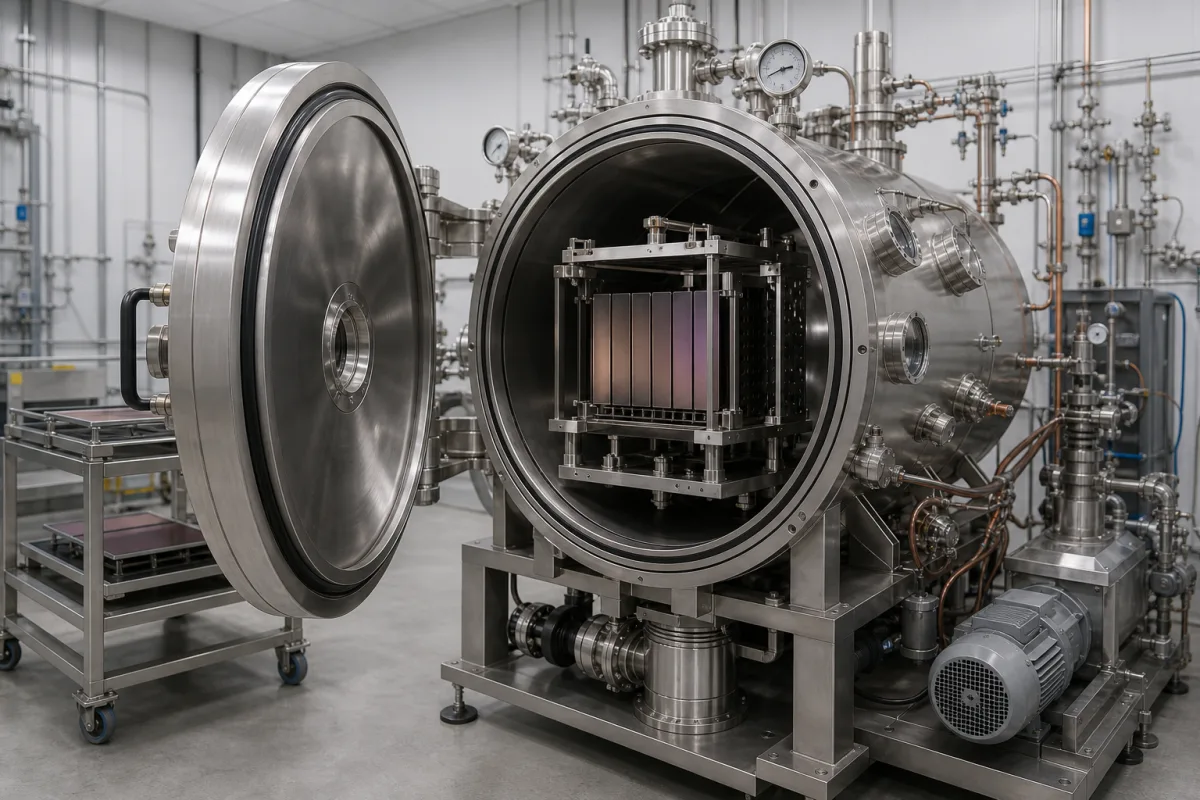
The image above shows a horizontal cylindrical chamber with its door open and a rack of coated panels inside, an arrangement for batch processing of flat substrates.
250 °C for 0, 10, 100 and 200 h; the authors call 200 h “promising a measure of uniform concentration of thallium”, and a 0.1 % Tl sample after 200 h gave about 40 % of the light intensity of a single crystal [2]
Thickness and light output
On graphite, relative light output 1, 2.8 and 4.3 at 70, 150 and 230 µm; on fibre optic plate 4.6, 7.4 and 8.7 [4]
Graphite gave the darkest image but higher MTF and NEQ; fibre optic plate the brightest image with the lowest MTF; silver-coated silica raised light output over plain silica [4]
Give the substrate type (glass, graphite, fibre optic plate, sensor panel), its size and heat limit, and whether the post-deposition anneal is done in the same chamber or a separate oven.
04
Chamber requirements for a CsI:Tl evaporation enquiry
Paste it into your enquiry below or into an email to a maker, then replace every bracket.
Layer: [thickness µm; columnar or dense; Tl mol%]
Substrate: [material; size; max temperature]
Pressure: [base; process; inert gas control]
Sources: [number of cells; max temperature; CsI charge g]
Holder: [heating range; rotation; distance to source]
Rate: [Å/s or µm/h]
Post-treatment: [anneal °C and hours; in situ or separate]
Explore company information and manufacturing capabilities, then discuss the scope of your project with a relevant supplier.
Share this page
Compiled and source-reviewed by the CNFX editorial team.
Each manufacturer above links to the page on that company's own website where the product is listed, with the date we checked it. How we source and review
· Page last updated 13 October 2026
Buyer questions
What pressure is used to grow columnar CsI:Tl?
NanoFocusRay and KAIST obtained needle-shaped columns at 10⁻² Torr with a 150 °C substrate, and a dense structure with cracks at 10⁻⁵ Torr. [1]
Why are CsI and thallium iodide evaporated from separate sources?
TlI melts at 440 °C and CsI at 660 °C, and the KAIST group writes that in a simple process TlI is “supposed to be evaporated before CsI powder melts”; BINP found Tl adequate only below 10 µm in a single-boat process. [2][3]
Is CsI:Tl heat-treated after evaporation?
Yes in these studies: NanoFocusRay and KAIST used 250 to 400 °C for 2 h 30 min, and KAIST reported that 200 hours at 250 °C was promising for a uniform thallium distribution. [1][2]
Sources and what still needs a direct check
Sources checked 2026-10-13. Four research reports from three publishers: two Korean Nuclear Society conference papers (NanoFocusRay with KAIST, 2011; KAIST), the Budker Institute's paper in the CERN proceedings (2017), and the Institute of High Energy Physics paper on CsI(Tl) substrates (arXiv).