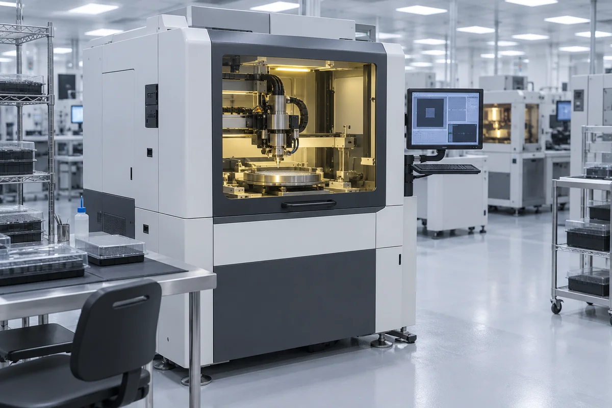
Select a die bonder around the die, substrate and joining process. A camera can locate a feature accurately while the completed bond still needs its own acceptance test. This guide compares the HM-IM’s published web and brochure specifications, follows its handling and bonding modules, and separates adhesive-process guidance from equipment ratings.
CNFX editorial research · Sources checked October 10, 2026 · 8 sources
Follow the die from its carrier to the bonded substrate
The HM-IM brochure shows blue-tape wafer feeding, CCD alignment, Z-axis closed-loop force control and pulse temperature control. Its nozzle and heating modules change with the joining process; obtain the configuration drawing for the supplied machine. [2]
Functional assembly / BOM reference
Work performed
Published configuration and missing detail
Wafer carrier and feeding
Present dies to the pickup station.
The brochure illustrates automatic blue-tape wafer feeding; the web page lists four wafer diameters. Carrier, tape, die-release and ejector compatibility need confirmation for the actual thin or fragile die. [2][1]
Pickup nozzle and vacuum system
Hold and transfer the selected die.
The brochure lists chip pickup nozzles and a vacuum/pneumatic system. The web page offers custom nozzles. Neither gives a nozzle material grade or vacuum setting for your die. [2][1]
Bonding head and force control
Place the die and apply the selected bond load.
The brochure shows Z-axis closed-loop control and interchangeable heated/ultrasonic modules. Its force range differs from the web page; identify the installed head and force sensor. [2][1]
Optical alignment and inspection
Locate features for placement and monitor the process.
CCD imaging, closed-loop vision and an optional side-view camera are listed. Imaging resolution is a different specification from final placement error. [2][1]
Substrate fixture, stage and motion
Support the substrate and move the die/tool to the working position.
The brochure lists substrate stages, an XYZ fine-tuning fixture, marble platform and anti-vibration frame among configurable modules. Obtain the axis layout and fixture envelope; “positioning accuracy” does not specify each stage’s travel or repeatability. [2]
Heating stage and heated nozzle
Deliver the recipe’s thermal input at the substrate or tool.
Pulsed bottom heating, top heating, constant-temperature and pulse controllers are listed. Confirm which module the temperature range and ramp rate describe. No heater-block material is specified. [2][1]
Dispensing / dipping and cure modules
Apply the selected attach medium and perform the specified cure step.
Glue dispensing/dipping, a side-dispenser controller and UV curing are listed. Module inclusion, adhesive compatibility, deposit control and cure verification require a process-specific quotation. [2]
Functional structure, not a production bill of materials with certified grades or quantities. For service, request nozzle and fixture references, cleaning compatibility, vision/force/temperature calibration procedures and replacement-part instructions for the supplied modules.
02
Read the accuracy figures carefully
Himalaya Semiconductor publishes its HM-IM fully automatic die bonder for R&D, pilot production and small batches, with these specifications [1].
Three different accuracy numbers
The web page specifies ≤3 µm placement accuracy and 0.5 µm imaging resolution. PDF page 3 instead states ±0.5 µm positioning accuracy for a closed-loop vision system; page 5 labels an illustration simply “Precision 0.5µm”. These descriptions do not define the same test. None states a 3σ basis. Request X/Y/rotation results, sample size, measurement method and pre- or post-bond condition. [1][2]
Resolve the range conflicts before ordering tooling
PDF page 5 prints chip size 0.25–40 mm, substrate size 0.5–140 mm and bonding “pressure” 0.01–500 N. The web page instead gives die dimensions 0.4×0.4 to 30×30 mm, a 100×200 mm work area and 0.1–30 N bond force. The PDF’s N value is a force, not pressure per area. Do not combine the largest ranges into one configuration; request a dated model/module schedule. [1][2]
Wafer diameter, individual die dimensions, substrate dimensions and usable work area are separate interfaces. The 450°C maximum and ±1°C claim also need a specified measurement location, module and load. [1]
03
Match the process modules to the product
The HM-IM is modular; the maker lists these processes and applications [1][2].
Changeover is the main trade-off
Himalaya promotes quick module changeover for R&D, pilot and small-batch work. Its comparison with “conventional” bonders is the maker’s positioning, not a comparative trial. The page gives no units-per-hour figure; time a complete recipe with feeding, recognition, dispense, heating and unloading. [1]
Adhesive die bonding
Epoxy or silver paste dispensing or dipping; IC packaging, MEMS, LEDs, sensors [1]
Face-to-face bonding for advanced packaging, chiplets, SiP [1]
Thermal compression
The brochure lists a high-frequency top-heating module with AuSn or solder preforms; the web page lists fine-pitch assembly and die stacking as applications. Confirm the exact joining mechanism and recipe rather than treating those material names as a complete thermocompression specification. [1][2]
Epoxy Technology’s Tech Tip 6 gives general guidance on cure and bond-line thickness. Use the selected adhesive’s technical data sheet and a validated assembly process for the actual requirement; the note is not an HM-IM capability specification. [3]
Adhesive category in Tech Tip 6
Published guidance
Application boundary
Silver-filled
12 µm minimum; the note pairs this with 0.5 mil and suggests 1–3 mil as ideal.
A general die-attach/SMD guideline. The paired metric/imperial figures are rounded; confirm the selected grade’s requirement. [3]
Thermally conductive, non-silver
25–75 µm (1–3 mil).
Guidance for heat sinking/potting; not a universal die-attach setting. [3]
Optical / UV-cured
3 µm in fibre-optic applications.
Do not transfer this value to every UV adhesive or to silver-filled die attach. [3]
Too thin
The note lists mechanical, electrical, thermal and optical problems that can arise when a bond line is too thin. It is not a model predicting resistance from thickness alone. [3]
Cure temperature
The minimum cure temperature applies to the bond line itself, not the oven or hot plate setting; allow for thermal lag [3]
Control
Use spacers, shims or dispensing control to hold bond-line thickness [3]
Record the adhesive grade, dispensing pattern/volume, bond force, target thickness and actual cure conditions together. A programmed heater setpoint alone does not show that the adhesive reached its required cure temperature. [3]
05
Prove alignment and bond strength
Use recognition trials to check whether the machine finds real production parts, then a separate bond test to assess the assembled joint. Placement and die shear measure different outcomes.
Vision must cope with real parts
Palomar’s pattern-recognition note describes problems caused by scratches, contamination and angled presentation in pixel-to-pixel matching. Raising a recognition threshold can also reject more parts. Trial representative dies and record recognition failures, false accepts and manual interventions; this source does not show which algorithm HM-IM uses. [4]
Name the strength test
MIL-STD-883-2 with Change 1 (12 January 2022), Method 2019.11, assesses die-attach integrity using applied force, failure mode and the appearance of residual attach material. It is a microcircuit test method, not certification of a bonder. Name the applicable method/revision, device construction, sampling and acceptance conditions in the acquisition document. [5]
X/Y/rotation measurements after the agreed bonding/cure/reflow process, with sample count and measurement uncertainty.
Bond-line thickness and the agreed void/coverage inspection method; do not equate dispense volume alone with verified coverage.
Die-shear results with the force, separation category and residual attach appearance required by the applicable acceptance plan. [5]
Demonstrate the proposed data export: the HM-IM brochure lists parameter/image recipes, report generation and traceability, but does not specify the complete per-part record or interface. [2]
06
Specify the test conditions and the installation interfaces
The following fields cover the placement process and the equipment installation. A value absent from the cited HM-IM documents is a quotation requirement, not a licence to borrow it from another bonder.
Parameter
Evidence available
Define in the quotation or acceptance plan
Placement accuracy · µm
Web ≤3 µm; PDF positioning ±0.5 µm, without a shared test basis. [1][2]
X/Y/rotation, statistical definition, sample size, reference features and measurement after the agreed joining cycle.
Throughput · units/hour
No sustained output stated in these HM-IM documents.
Good completed assemblies per hour for the selected recipe, including stops/rejects and manual loading.
Bond force · N
Web 0.1–30 N with 0.05 N resolution; PDF graphic 0.01–500 N. [1][2]
Installed head range, calibration, uncertainty and force/time profile. Resolution does not establish force accuracy.
Process temperature · °C
Web maximum 450°C, ±1°C and up to 10°C/s; top/bottom controllers are separate modules. [1][2]
Sensor location, tool/substrate/adhesive temperature, ramp and dwell under the specified load.
Die size and thickness · mm / µm
Web 0.4×0.4–30×30 mm and 70–1,100 µm thickness; PDF size range differs. [1][2]
Length and width separately, thickness, fragile features, carrier and compatible pickup tool; area alone is insufficient.
Vision resolution
Web imaging resolution 0.5 µm; no camera pixel count given. [1]
Object-space resolution, field of view, lighting and recognition test; do not convert µm to pixels without optical data.
Substrate size · mm
Web work area 100×200 mm; PDF substrate range 0.5–140 mm. [1][2]
Substrate dimensions/height, fixture and accessible bonding area; reconcile the two labels.
Cycle time · seconds
No complete HM-IM cycle time specified.
Define cycle start/end, number of dies, vision attempts, dispensing, thermal dwell and unload time.
Electrical supply · V / Hz / phases
Web offers electrical documentation but gives no supply rating. [1]
Selected modules, rated/peak consumption and facility supply; do not assume a three-phase option.
Himalaya publishes a modular die-bonder platform; Minder lists automatic bonders with manual loading and unloading. The other profiles below describe motion controls, sensors or a chip maker’s own packaging equipment. Use the stated role to choose a relevant contact.
Jiangsu Himalaya Semiconductor Co., Ltd.
Suzhou, Jiangsu (contact region; model plant to be verified), CN
HM-IM is presented for R&D, pilot and small-batch assembly, with configurable bonding processes. Web and brochure force/die-size ranges differ; request one dated specification identifying the head, heater, tooling and acceptance test.
MD-JC360 and MD-JC380 are listed as automatic die bonders for 8-inch and 12-inch wafers respectively, with manual loading and unloading. Ask for the exact process, accuracy test and sustained cycle data; “automatic” here does not mean unattended carrier handling.
Supplies motion control to die-bonder builders, including servo drives and motor/control integration. Relevant when specifying or upgrading the bonder's motion system.
Supplies sensors used inside die bonders: wafer and substrate presence detection, vision and displacement sensing. Relevant for sensing upgrades and spares.
Explore company information and manufacturing capabilities, then discuss the scope of your project with a relevant supplier.
Share this page
Compiled and source-reviewed by the CNFX editorial team.
The linked sources support the stated equipment or application role on each record. A controls case or an in-house production line is not evidence of complete die-bonder manufacture. How we source and review
· Page last updated 13 October 2026
Buyer questions
Is imaging resolution the same as placement accuracy?
HM-IM’s web page lists 0.5 µm imaging resolution and ≤3 µm placement accuracy, while its brochure states ±0.5 µm positioning accuracy. They have different labels and no shared published test basis. Specify the measured outcome after your agreed joining process. [1][2]
How thin can a silver epoxy die-attach bond line be?
Epoxy Technology’s general note suggests a 12 µm minimum, paired with 0.5 mil, and an ideal 1–3 mil range for silver-filled adhesives. These are rounded general guidelines; use the selected adhesive data sheet and validate the bond line in your assembly. [3]
What bonding processes can one die bonder run?
HM-IM lists adhesive, eutectic, flip-chip, thermocompression and UV modules. Confirm which head, heater, atmosphere and fixtures are included. Its brochure and web force/die-size ranges differ, so the list does not prove one configuration covers all extremes. [1][2]
Which standard covers die shear testing?
MIL-STD-883-2 with Change 1, dated 12 January 2022, includes Method 2019.11 for die shear. It evaluates force, failure mode and residual attach appearance. Its use in an acceptance plan does not certify the die bonder. [5]
Sources and what still needs a direct check
Sources checked 2026-10-10. Standards bodies and regulations define the requirements; manufacturer pages show published ranges for those models only. CNFX does not certify products or suppliers.