Editorial Technical Reference

Automated Optical Inspection Unit

This page explains how Automated Optical Inspection Unit is classified within Computer, Electronic and Optical Product Manufacturing. Technical values and manufacturer relationships are research references; confirm the current specification and supplier evidence for each order.

Technical Definition & Core Assembly

A vision-based inspection component that automatically detects defects on printed circuit boards during assembly.
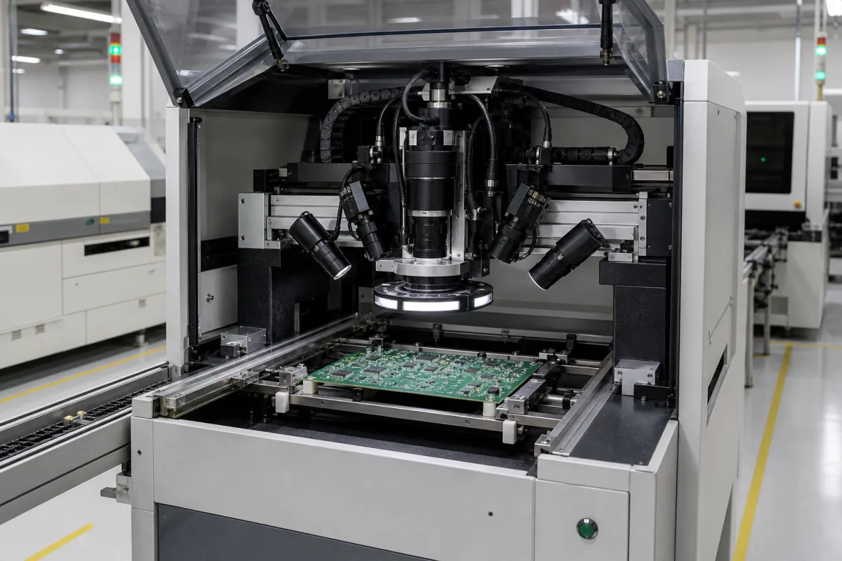
Representative product image. Confirm appearance and specifications with the manufacturer.

Product Specifications

Technical details and manufacturing context for Automated Optical Inspection Unit

Definition
An Automated Optical Inspection Unit is a critical component within a Modular Printed Circuit Board Assembly System. It uses high-resolution cameras, controlled lighting, and image processing algorithms to automatically inspect PCBs for manufacturing defects such as missing components, misalignment, solder bridges, and component polarity errors during the assembly process. The unit captures images of the PCB from multiple angles, and software compares these against reference designs or golden samples to identify deviations. Machine learning algorithms may be employed to classify defect types and severity. The unit is typically integrated into a production line, where it performs inline inspection at various stages. Its inspection area ranges from 300 to 500 mm × mm, with a resolution of 10–25 µm/pixel, allowing detection of fine defects. Inspection speed is 0.5–2.0 m²/min, balancing throughput with resolution. Detection accuracy is ±0.05 mm, and the false call rate is ≤0.5%. The lighting operates in the visible spectrum (450–650 nm), with optional UV/IR. Power supply is 220 V AC ±10%, with consumption of 1.5–3.0 kW. Operating temperature is 10–40 °C, humidity 20–80% RH non-condensing, and ingress protection is IP54–IP65 per IEC 60529. The unit weighs 800–1200 kg. Materials include an aluminum alloy frame, optical glass lenses, LED lighting arrays, and electronic circuit boards. This directory entry provides reference values; actual specifications must be confirmed with the legal manufacturer for the specific model and application.
Working Principle
The unit captures high-resolution images of PCBs using multiple cameras under controlled lighting conditions. Image processing software compares the captured images against reference designs or golden samples to identify deviations and defects. Machine learning algorithms may be employed to classify defect types and severity. The system uses visible light (450–650 nm) and can achieve a resolution of 10–25 µm/pixel. The inspection area is 300–500 mm × mm, and the speed is 0.5–2.0 m²/min. Detection accuracy is ±0.05 mm, with a false call rate of ≤0.5%. The unit operates within 10–40 °C and 20–80% RH, and is protected to IP54–IP65.
Common Materials
Aluminum alloy frame, Optical glass lenses, LED lighting arrays, Electronic circuit boards
Technical Parameters
ParameterTypical rangeNotes & selection driver
Inspection Area300–500 mm × mmMaximum PCB size that can be inspected in one pass.
Resolution10–25 µm/pixelHigher resolution detects finer defects but reduces throughput.
Inspection Speed0.5–2.0 m²/minAffects line cycle time; balance with resolution.
Detection Accuracy±0.05 mmPositional accuracy of defect location.
False Call Rate≤0.5 %Percentage of good boards flagged as defective; lower is better.
Lighting Wavelength450–650 nmVisible spectrum; may include UV/IR options.
Power Supply220 ±10% V ACSingle phase; other voltages on request.
Power Consumption1.5–3.0 kWDepends on lighting and computer configuration.
Operating Temperature10–40 °COutside range may affect accuracy.
Humidity20–80 % RHNon-condensing.
Ingress ProtectionIP54–IP65Protection against dust and water jets.IEC 60529
Weight800–1200 kgIncluding base and enclosure.

Ranges are indicative industry figures for RFQ preparation, not a supplier commitment. Confirm every value and standard with the legal manufacturer before ordering.

Components / BOM
  • Camera Array
    Captures high-resolution images of PCB surfaces from multiple angles
    Material: Aluminum housing with optical glass
  • Lighting System
    Provides controlled illumination for optimal image capture and defect detection
    Material: LED arrays with diffusers
  • Image Processing Unit
    Processes captured images and compares against reference designs to identify defects
    Material: Electronic circuit boards with processors
  • Mechanical Positioning System
    Precisely positions cameras and lighting relative to the PCB
    Material: Steel and aluminum with linear guides

Industrial Ecosystem & Supply Chain Structure

Complementary Systems
Downstream Applications
Specialized Tooling

Application Fit & Sizing Matrix

Operational Limits
pressure: Atmospheric (no pressure requirements)
other spec: Humidity: 30-70% RH non-condensing, Vibration: <0.5G, Illumination: Controlled ambient lighting required
temperature: +10°C to +40°C
Media Compatibility
✓ FR-4 PCB substrates ✓ Solder mask coatings ✓ Surface mount components (SMDs)
Unsuitable: High-vibration environments without isolation
Sizing Data Required
  • PCB maximum dimensions (LxW)
  • Minimum defect size to detect (in microns)
  • Required inspection speed (boards per hour)

Reliability & Engineering Risk Analysis

Failure Mode & Root Cause
Lens Contamination
Cause: Accumulation of dust, oil mist, or debris on optical components, degrading image quality and inspection accuracy due to inadequate environmental sealing or infrequent cleaning.
LED Array Degradation
Cause: Gradual loss of illumination intensity or color shift in lighting elements, often from thermal stress, prolonged operation, or power supply fluctuations, leading to inconsistent inspection results.
Maintenance Indicators
  • Increased false reject rates or inspection errors in quality reports
  • Unusual audible vibrations or grinding noises from moving parts (e.g., conveyors, cameras)
Engineering Tips
  • Implement a scheduled cleaning regimen for lenses and lighting with approved materials, and maintain controlled environmental conditions (temperature, humidity, cleanliness) around the unit.
  • Use predictive maintenance tools like vibration analysis for mechanical components and monitor LED output with photometers to schedule proactive replacements before failure.

Indicative industry ranges for design and RFQ preparation. Confirm the exact figures and applicable standard with the manufacturer before specifying.

Compliance & Manufacturing Standards

Applicable Standards
CE Marking - Directive 2014/35/EU (Low Voltage Directive) ASTM E1316-24 - Standard Terminology for Nondestructive Examinations

Quoted from the published standard.

Manufacturing Precision
  • Resolution: +/-0.005mm
  • Repeatability: +/-0.01mm
Quality Inspection
  • Calibration Verification Test
  • Image Uniformity Test

Manufacturers of Automated Optical Inspection Unit

Manufacturer profiles associated with Automated Optical Inspection Unit.

Sourcing Automated Optical Inspection Unit from China?
Tell us your specification and target quantity — we will match it against manufacturer records and come back with the factories that fit.
Request manufacturers We manufacture this

Manufacturer listings support early research and capability understanding. They are not certification, ranking, or transaction guarantees.

Technical documentation
Request current drawings, revision history, and a signed specification sheet.
Manufacturing capability
Verify equipment lists, process limits, capacity, and representative production evidence.
Inspection readiness
Confirm test methods, calibrated equipment, sampling plans, and traceable reports.
Supplier transparency
Check the legal entity, factory address, ownership, certifications, and direct contacts.

CNFX does not score or rank suppliers. Buyers must verify all claims and documents with the legal manufacturer before ordering.

Supply Chain Compatible Machinery & Devices

Industrial IoT Gateway

The Industrial IoT Gateway is a ruggedized edge computing device designed for industrial environments.

Explore Specs →
Modular Industrial Edge Computing Device

This modular industrial edge computing device is a ruggedized system designed for deployment in harsh industrial environments to perform real-time data processing, analytics, and control functions at the network edge.

Explore Specs →
Industrial Smart Camera Module

The Industrial Smart Camera Module is a compact, self-contained vision processing unit designed for integration into industrial machinery and production lines.

Explore Specs →
Surface Mount Resistor

Passive electronic component for current limiting and voltage division in circuits

Explore Specs →

Frequently Asked Questions

What defects can this AOI unit detect?

It detects missing components, misalignment, solder bridges, and component polarity errors during PCB assembly, as described in the product definition.

What is the inspection area and resolution?

The inspection area is 300–500 mm × mm, and the resolution is 10–25 µm/pixel. Higher resolution detects finer defects but reduces throughput.

What are the environmental requirements?

Operating temperature is 10–40 °C, humidity 20–80% RH non-condensing, and ingress protection is IP54–IP65 per IEC 60529. These are reference values; confirm with the manufacturer.

How is the false call rate defined?

The false call rate is the percentage of good boards flagged as defective; the reference value is ≤0.5%. Lower is better. Verify the actual rate for your application.

Data Basis

Editorial classification, named public sources where available, and source-reviewed manufacturer records.

Preliminary Technical Classification
This page supports structured research, RFQ preparation, and supplier evaluation. It does not replace buyer-led supplier qualification, standards review, or technical approval.
Buyer enquiry

Request manufacturing insight for Automated Optical Inspection Unit

Ask for use case, specification boundaries, supplier type, and RFQ preparation information for this product.

Where it goes
Straight to the CNFX editorial desk, and to the manufacturer if this product is linked to a claimed profile. Nothing is broadcast to a supplier list.
Your details stay here
We do not sell or rent enquiry data, and we do not add you to a mailing list. Used only to answer this request.
No commission, no middleman
CNFX is a directory. We take no cut of any order and never negotiate on a supplier's behalf.
What we don't claim
A listing is not an endorsement. Qualify every supplier and verify every figure yourself before ordering.

Your business information is used only to process this request.

Thank you! Your message has been sent. We'll respond within 1–3 business days.
Sorry, we couldn't send your message. Please try again, or email us at contact@cnfx.com.

Need to Manufacture Automated Optical Inspection Unit?

Compare manufacturer profiles with relevant product and process capability.

Previous Product
XY Positioning Stage
Last Product
Get QuotesChat