Editorial Technical Reference

Low-Noise Amplifier (LNA)

This page explains how Low-Noise Amplifier (LNA) is classified within Computer, Electronic and Optical Product Manufacturing. Technical values and manufacturer relationships are research references; confirm the current specification and supplier evidence for each order.

Technical Definition & Core Assembly

An electronic amplifier that amplifies very weak signals while adding minimal additional noise.
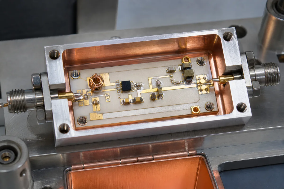
Representative product image. Confirm appearance and specifications with the manufacturer.

Product Specifications

Technical details and manufacturing context for Low-Noise Amplifier (LNA)

Definition
A low-noise amplifier (LNA) is a critical component within wireless radio modules, designed to amplify incoming radio frequency (RF) signals from antennas with minimal degradation of the signal-to-noise ratio. This enables reliable reception of weak signals in communication systems, such as cellular base stations, Wi-Fi routers, satellite receivers, and radar systems. The LNA is typically the first active stage in the receiver chain, and its noise performance largely determines the overall sensitivity of the system. By providing high gain while introducing as little noise as possible, the LNA ensures that subsequent stages can process the signal without being overwhelmed by noise. The device operates over a frequency range of 0.5 to 6 GHz, covering typical communication bands. It offers a gain of 15 to 25 dB, a noise figure of 0.5 to 1.5 dB, and input and output return losses greater than 10 dB, ensuring good impedance matching. The LNA requires a DC supply voltage of 3.3 to 5 V and consumes 20 to 80 mA of current. It can deliver an output power of 10 to 20 dBm at the 1 dB compression point, and can handle input power levels up to 10 to 20 dBm. The operating temperature range is -40 to 85°C, suitable for industrial environments. The component is available in a surface-mount device (SMD) package with dimensions ranging from 3×3 mm to 5×5 mm, facilitating compact integration. Typical materials include Gallium Arsenide (GaAs), Silicon Germanium (SiGe), and CMOS silicon, each offering different trade-offs in performance and cost. When selecting an LNA, engineers must verify model-specific parameters, such as exact frequency range, gain, noise figure, and supply voltage, against the intended application. It is essential to consult the manufacturer's datasheet and confirm compliance with any relevant standards, as the values provided here are reference ranges for a product category, not guaranteed specifications for a specific part.
Working Principle
The LNA operates by using transistors, typically made of GaAs, SiGe, or CMOS, in specific configurations to provide high gain while minimizing internal noise generation. The design involves careful impedance matching at the input and output to ensure maximum power transfer and minimal signal reflection. Biasing circuits set the operating point of the transistor to achieve low noise and high linearity. The transistor's noise figure is minimized by selecting appropriate device geometry and operating conditions. The circuit may include feedback networks to stabilize gain and improve bandwidth. The LNA amplifies the weak RF signal while adding minimal noise, preserving the signal-to-noise ratio for subsequent processing.
Common Materials
Gallium Arsenide (GaAs), Silicon Germanium (SiGe), CMOS Silicon
Technical Parameters
ParameterTypical rangeNotes & selection driver
Frequency Range0.5–6 GHzCovers typical communication bands
Gain15–25 dBHigher gain improves signal level
Noise Figure0.5–1.5 dBLower is better for weak signals
Input Return Loss>10 dBEnsures good matching
Output Return Loss>10 dBEnsures good matching
Supply Voltage3.3–5 V DCTypical for RF amplifiers
Current Consumption20–80 mAAffects power budget
Output Power (P1dB)10–20 dBmAt 1 dB compression point
Operating Temperature Range-40–85 °CIndustrial grade
Input Power Handling10–20 dBmMaximum safe input
Package TypeSMDSurface mount for compactness
Dimensions3×3–5×5 mmSmall footprint for integration

Ranges are indicative industry figures for RFQ preparation, not a supplier commitment. Confirm every value and standard with the legal manufacturer before ordering.

Components / BOM
  • Transistor Part
    Active amplification element that provides gain while minimizing noise
    Material: Gallium Arsenide or Silicon Germanium
  • Input Matching Network
    Optimizes impedance matching between antenna and amplifier input to minimize noise
    Material: Copper traces on PCB with passive components
  • Output Matching Network
    Matches amplifier output impedance to subsequent stages for maximum power transfer
    Material: Copper traces on PCB with passive components
  • Bias Circuit Part
    Provides stable DC operating conditions for the transistor
    Material: Resistors, capacitors, and inductors on PCB
  • Feedback Network Optional
    Trades a little gain for flatter bandwidth and better stability, on designs that use it.

Applied To / Applications

This component is essential for the following industrial systems and equipment:

Industrial Ecosystem & Supply Chain Structure

Complementary Systems
Downstream Applications
Specialized Tooling

Application Fit & Sizing Matrix

Operational Limits
pressure: Not applicable (solid-state electronic device)
other spec: Frequency range: 0.5-6 GHz, Noise figure: <1.5 dB typical, Gain: 20-30 dB typical, Power supply: 3-5 VDC
temperature: -40°C to +85°C (operational range)
Media Compatibility
✓ RF communication systems ✓ Satellite receivers ✓ Medical imaging equipment
Unsuitable: High-power RF environments without proper isolation
Sizing Data Required
  • Required frequency range (GHz)
  • Maximum acceptable noise figure (dB)
  • Required gain (dB)

Reliability & Engineering Risk Analysis

Failure Mode & Root Cause
Thermal degradation of semiconductor components
Cause: Excessive operating temperature due to inadequate heat dissipation, leading to material fatigue and performance drift.
Electrostatic discharge (ESD) damage to sensitive transistors
Cause: Improper handling during installation or maintenance, causing irreversible breakdown of gate oxides or junctions.
Maintenance Indicators
  • Audible: Sudden increase in background noise or distortion in output signal.
  • Visual: Abnormal heat emission detected via thermal imaging, indicating potential thermal runaway or component failure.
Engineering Tips
  • Implement strict ESD protection protocols during all handling and maintenance activities, including use of grounded workstations and wrist straps.
  • Ensure optimal thermal management through regular cleaning of heat sinks, verification of cooling system integrity, and monitoring of operating temperatures with calibrated sensors.

Indicative industry ranges for design and RFQ preparation. Confirm the exact figures and applicable standard with the manufacturer before specifying.

Compliance & Manufacturing Standards

Applicable Standards
CE Marking (EU Directive 2014/53/EU for Radio Equipment)

Quoted from the published standard.

Manufacturing Precision
  • Gain Flatness: +/-0.5 dB across frequency band
  • Input/Output Impedance: 50 ohms +/-5%
Quality Inspection
  • Noise Figure Measurement Test
  • Third-Order Intercept Point (IP3) Test

Manufacturers of Low-Noise Amplifier (LNA)

Manufacturer profiles associated with Low-Noise Amplifier (LNA).

Sourcing Low-Noise Amplifier (LNA) from China?
Tell us your specification and target quantity — we will match it against manufacturer records and come back with the factories that fit.
Request manufacturers We manufacture this

Manufacturer listings support early research and capability understanding. They are not certification, ranking, or transaction guarantees.

Technical documentation
Request current drawings, revision history, and a signed specification sheet.
Manufacturing capability
Verify equipment lists, process limits, capacity, and representative production evidence.
Inspection readiness
Confirm test methods, calibrated equipment, sampling plans, and traceable reports.
Supplier transparency
Check the legal entity, factory address, ownership, certifications, and direct contacts.

CNFX does not score or rank suppliers. Buyers must verify all claims and documents with the legal manufacturer before ordering.

Supply Chain Compatible Machinery & Devices

Industrial IoT Gateway

The Industrial IoT Gateway is a ruggedized edge computing device designed for industrial environments.

Explore Specs →
Modular Industrial Edge Computing Device

This modular industrial edge computing device is a ruggedized system designed for deployment in harsh industrial environments to perform real-time data processing, analytics, and control functions at the network edge.

Explore Specs →
Industrial Smart Camera Module

The Industrial Smart Camera Module is a compact, self-contained vision processing unit designed for integration into industrial machinery and production lines.

Explore Specs →
Surface Mount Resistor

Passive electronic component for current limiting and voltage division in circuits

Explore Specs →

Frequently Asked Questions

What is the typical frequency range of an LNA?

The typical frequency range for this LNA category is 0.5 to 6 GHz, covering common communication bands. However, the exact range depends on the specific model, so always check the datasheet.

How does the noise figure affect system performance?

A lower noise figure means the LNA adds less noise to the signal, which is critical for receiving weak signals. The reference range is 0.5 to 1.5 dB, but the actual value varies by model and must be verified.

What supply voltage is required?

The LNA typically operates with a DC supply voltage of 3.3 to 5 V. Confirm the exact requirement from the manufacturer's specifications for the specific part.

Can this LNA be used in outdoor applications?

The operating temperature range is -40 to 85°C, which is suitable for many industrial environments. However, for extreme conditions, verify the model's ratings and any additional environmental protections needed.

Data Basis

Editorial classification, named public sources where available, and source-reviewed manufacturer records.

Preliminary Technical Classification
This page supports structured research, RFQ preparation, and supplier evaluation. It does not replace buyer-led supplier qualification, standards review, or technical approval.
Buyer enquiry

Request manufacturing insight for Low-Noise Amplifier (LNA)

Ask for use case, specification boundaries, supplier type, and RFQ preparation information for this product.

Where it goes
Straight to the CNFX editorial desk, and to the manufacturer if this product is linked to a claimed profile. Nothing is broadcast to a supplier list.
Your details stay here
We do not sell or rent enquiry data, and we do not add you to a mailing list. Used only to answer this request.
No commission, no middleman
CNFX is a directory. We take no cut of any order and never negotiate on a supplier's behalf.
What we don't claim
A listing is not an endorsement. Qualify every supplier and verify every figure yourself before ordering.

Your business information is used only to process this request.

Thank you! Your message has been sent. We'll respond within 1–3 business days.
Sorry, we couldn't send your message. Please try again, or email us at contact@cnfx.com.

Need to Manufacture Low-Noise Amplifier (LNA)?

Compare manufacturer profiles with relevant product and process capability.

Previous Product
Loop Filter
Next Product
Main Control Unit (MCU)
Get QuotesChat