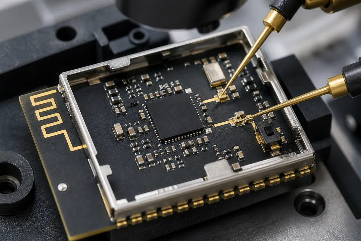
Board-level design around a 2.4 GHz transceiver chip
The illustration shows a transceiver chip in a QFN package inside an open shield frame, with its crystal, a row of 0201-size parts, a meandered PCB antenna at the board end and two RF probes touching the trace between chip and antenna. Those probes mark where board-level work on a radio concentrates: the chip's datasheet performance only appears if the matching network, the antenna and the reference crystal are right for that particular board.
Covers the circuit and layout around an RF transceiver IC on a product or module board: 50 Ω RF traces, chip-side and antenna-side matching networks and their tuning by S-parameters, harmonic suppression, copying a reference PCB antenna and its ground clearance, reference crystal tolerance, load capacitance and frequency-offset trimming, and layout faults that degrade transmit EVM or receive sensitivity. Choosing transceiver chips is on RF integrated circuit (RFIC); end-of-line production RF testing of modules is on Wireless communication module; pre-certified modules are on Wireless module; RF multicouplers and duplexers are outside this page.
CNFX editorial research · Sources checked October 12, 2026 · 4 sources
Espressif's ESP32 hardware design guidelines describe the RF path as three parts: 50 Ω controlled-impedance RF traces, a chip-side matching circuit, and the antenna with its own matching circuit.
The chip-side match sits close to the chip, preferably as a CLC structure, which sets the impedance point and suppresses harmonics. Matching values vary from board to board, so the values in a reference module cannot simply be reused. Tuning is done with a network analyser across the two ends of the network: port 1 at the chip, port 2 toward the antenna. The target is S11 close to the chip's conjugate point of 25 + j0 Ω, with S21 below −35 dB at 4.8 GHz and 7.2 GHz, the second and third harmonics of 2.4 GHz.
If the layout follows Espressif's reference, the starting ranges are C11 1.2–1.8 pF, L2 2.0–3.0 nH and C12 1.2–1.8 pF, in 0201 packages, with a stub on the first capacitor at the chip end. A second CLC network near the antenna is recommended for antenna tuning unless simulation guarantees the antenna is at 50 Ω, plus ESD protection on the antenna.
Measurement
Target (Espressif ESP32)
S11 at the chip port
Close to the conjugate point 25 + j0 Ω
S21 at 4.8 GHz (2nd harmonic)
< −35 dB
S21 at 7.2 GHz (3rd harmonic)
< −35 dB
RF trace
50 Ω, outer layer, no vias, 135° bends or arcs, solid ground on the adjacent layer
The harmonic labels (2 × and 3 × 2.4 GHz) are an editorial reading. Ask for the S11/S21 plots of the tuned network on the production board, not the reference board.
02
Copying a reference PCB antenna
TI's application note AN043 (SWRA117D) documents the meandered inverted-F antenna on its CC2511 USB dongle reference design.
The antenna fits in 15.2 × 5.7 mm and was designed to match 50 Ω at 2.45 GHz without matching components. The design goal was reflection below −10 dB (VSWR below 2) across the 2.4 GHz band, which delivers more than 90% of available power to the antenna. TI measured gains of 4.5 to 5.3 dB in free space and 3.3 dB with the dongle plugged into a laptop, and a line-of-sight range of 240 m at 250 kbps and 1% packet error rate.
TI's rule for reuse is strict: small changes in antenna dimensions can have a large effect, so make an exact copy, ideally by importing its Gerber or DXF file and overlaying the result to check it, use the same PCB thickness and material, and lengthen or shorten the antenna slightly if the board is thinner or thicker. TI also notes that reflection measurements on so small an antenna with a small ground plane are affected by where the coax cable is soldered.
Espressif adds placement rules for module antennas: feed point near the board edge, base board cut away on both sides of and below the antenna, no module placed mid-board with clearance hollowed out on all four sides, and plenty of ground copper and vias near the feed.
Ask which reference antenna was copied, whether the substrate matches the reference, and for a measured S11 of the antenna on the final board in its enclosure.
03
Crystal tolerance, load capacitance and trimming
The reference crystal sets the carrier; an offset between transmitter and receiver pushes part of the signal outside the receive filter.
Cypress's patent US 7,787,829 B1 works through the numbers for a 2.4 GHz radio with 1 MHz channels and 900 kHz occupied bandwidth: a 50 ppm offset at 2,450 MHz is 122.5 kHz, which pushes 7.2% of the transmitted signal into the adjacent channel, and the patent puts 50 ppm as roughly the maximum a 2.4 GHz system tolerates without significant impact. It notes a crystal can drift, for example from +25 ppm to +65 ppm over five years at another temperature, and that meeting ±25 ppm can need a 10 ppm crystal costing 3 to 5 times as much as a 30 ppm one. Trimming the initial frequency with a digitally controlled capacitance, measured at manufacturing test and stored in non-volatile memory, removes the initial tolerance and lets 15 ppm crystals be used with a good share of 2.4 GHz radio ICs without impacting radio performance.
Espressif's ESP32 checklist asks for a 40 MHz crystal within ±10 ppm and sizes the load capacitors from C_L = C1·C2/(C1 + C2) + C_stray, with C_L from the crystal datasheet. The values are then adjusted on the real board: transmit a tone, read the frequency offset on an analyser, and bring it within ±10 ppm; a positive offset means the load capacitance is too small and needs increasing, a negative one the reverse. It also recommends a series inductor on XTAL_P, starting at 0 Ω, to reduce crystal harmonics reaching the RF, and crystal amplitude above 500 mV.
Offset at 2,450 MHz
Frequency error
±10 ppm
±24.5 kHz
±25 ppm
±61.25 kHz
±50 ppm
±122.5 kHz (patent example)
The 10 and 25 ppm rows are Editorial calculations (2,450 MHz × ppm). Example: a crystal with C_L = 10 pF on a board with 3 pF stray needs C1 = C2 = 14 pF to start (Editorial calculation, assumed values); then trim on the board.
04
Layout faults and their symptoms
Espressif's layout guide ends with symptoms seen on real boards and their causes.
The guide's crystal rules: ground-via stitching around the clock trace, no vias on the clock traces, series parts at the chip side, load capacitors on either side of the crystal near the end of the clock trace, and no high-frequency digital traces under the crystal.
Symptom
Cause given
Fix given
Transmit power far above or below target, poor EVM
Impedance mismatch between RF pin and antenna, driving the internal PA into saturation
Match the antenna to the chip with a π-type network on the RF trace
Good transmit, low receive sensitivity
External coupling into the antenna: crystal harmonics, UART traces crossing the RF trace, other high-frequency sources
Keep the antenna away from the crystal; keep high-frequency traces away from the RF trace
Crystal malfunction
High-frequency traces such as UART routed under the crystal; nearby inductors or antennas
Re-lay the crystal area
Ask for conducted transmit power, EVM and receive sensitivity measured on the production board, and the layout review checklist used.
05
What to agree for a transceiver board design
Paste it into your enquiry below or into an email to a maker, then replace every bracket.
Name the transceiver chip and bands, the antenna type (PCB copy of a named reference, chip antenna or connector), PCB stack-up and material, enclosure, and the target conducted power, EVM and sensitivity. Ask for the tuned matching values with S11/S21 plots, the antenna S11 on the final board, the crystal part with tolerance, load capacitance and measured frequency offset, whether trimming is used, and the layout review against the chip maker's guidelines.
Explore company information and manufacturing capabilities, then discuss the scope of your project with a relevant supplier.
Share this page
Compiled and source-reviewed by the CNFX editorial team.
Each manufacturer above links to the page on that company's own website where the product is listed, with the date we checked it. How we source and review
· Page last updated 13 October 2026
Buyer questions
What should the matching network achieve?
For ESP32, Espressif targets S11 close to the 25 + j0 Ω conjugate point and S21 below −35 dB at 4.8 and 7.2 GHz, tuned on the actual board with a network analyser. [3]
Can a reference PCB antenna be redrawn to fit?
TI says small dimension changes can have a large effect; copy it exactly, ideally from the Gerber or DXF file, on the same PCB material and thickness. [1]
How accurate must the crystal be?
Espressif asks for ±10 ppm on the ESP32's 40 MHz crystal; Cypress's patent notes 50 ppm at 2,450 MHz is 122.5 kHz and about the maximum a 2.4 GHz system tolerates. [3][2]
Why is receive sensitivity poor when transmit is fine?
Espressif attributes it to coupling into the antenna, such as crystal harmonics or UART traces crossing the RF trace. [4]
Sources and what still needs a direct check
Sources checked 2026-10-12. Two chip makers' design documents and a third chip maker's patent.