Receive noise chain, T/R isolation and compartment shielding
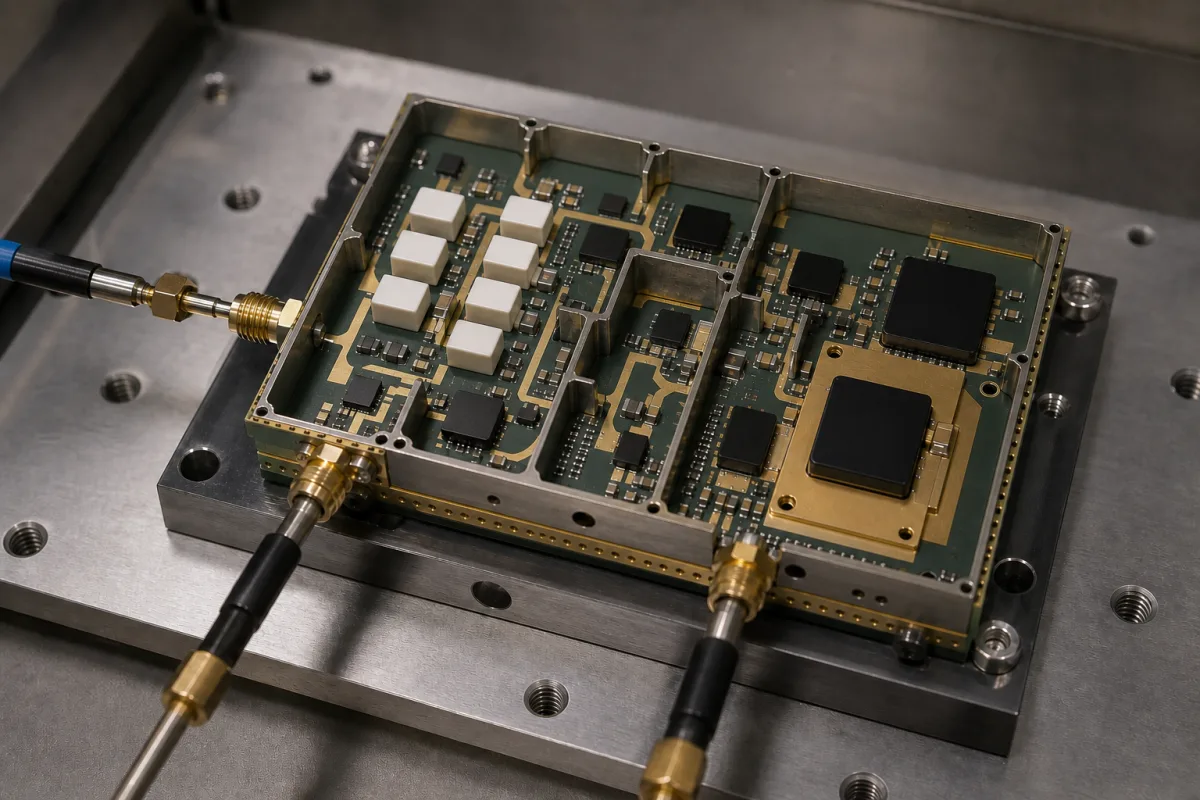
The front end in the illustration sits in a milled metal housing divided into compartments: ceramic filters in one bay, small amplifier and switch chips in others, a larger device on a gold heat spreader, and SMA connectors with test cables at the edges. A front-end module takes the transceiver's weak transmit signal up to antenna power and the antenna's weak receive signal up past the transceiver's own noise. Its numbers only make sense as a chain, and its housing is part of the circuit.
Covers RF front-end modules and front-end assemblies between transceiver and antenna: power amplifier, low-noise amplifier with bypass, T/R switch, filters and detector; the noise figure cascade and the cost of loss ahead of the LNA; transmit-to-receive isolation; PA thermal grounding; and compartment shielding and cavity resonance in the housing. Choosing transceiver and front-end chips is on RF integrated circuit (RFIC); stand-alone LNAs and the basic cascade effect of LNA gain are on Low-noise amplifier (LNA); matching networks, PCB antennas and crystals around a transceiver are on RF transceiver; broadband modulator driver amplifiers are on RF driver amplifier for electro-optic modulators.
CNFX editorial research · Sources checked October 12, 2026 · 3 sources
Inside a front-end module the LNA rarely sees the antenna directly: a T/R switch, and in some designs a filter, sit ahead of it, and the LNA can be bypassed. Agilent (now Keysight) Application Note 57-1 supplies the rule for costing both.
The cascade noise equation is F_sys = F1 + (F2 − 1)/G1 + (F3 − 1)/(G1·G2) + … . When the first element is a passive loss, G1 is below 1, so it amplifies the following stages' contribution instead of shrinking it. The note also warns that when the first stage has low gain, mismatch errors in the second stage become significant, which applies to a lossy filter or a bypassed LNA at the front.
Skyworks' SKY85329-11, a 2.4 GHz 802.11n front-end module with PA, LNA with bypass, SPDT T/R switch and power detector in a 2.5 × 2.5 mm QFN, lists receive gain of 16.5 dB typ. with the LNA on and −4.5 dB in bypass, and noise figure 2.1 dB typ. (2.4 dB max) from the antenna pin to the RX pin at 5 V. Skyworks says the LNA raises receive sensitivity or overcomes the loss of filters fitted ahead of it.
Chain (antenna → transceiver)
System noise figure
FEM, LNA on (NF 2.1 dB, G 16.5 dB) → transceiver NF 6 dB
≈2.3 dB
1.5 dB ceramic filter → same FEM → transceiver
≈3.8 dB
FEM in bypass (loss 4.5 dB) → transceiver NF 6 dB
≈10.5 dB
Editorial calculation with the cascade equation. The 6 dB transceiver noise figure and 1.5 dB filter loss are assumptions; a passive loss is taken to have a noise figure equal to its loss. Loss ahead of the LNA adds to system noise figure almost dB for dB, while loss after it is divided by the LNA gain. Ask for the noise figure from the module's antenna port, including any filter, at your band edges.
02
Transmit power at the receive port
In a time-division front end the T/R switch is all that stands between the PA and the LNA input during transmit.
At +25 dBm out and 48 dB typ. isolation, about −23 dBm reaches the RX pin; at the 40 dB minimum, about −15 dBm (Editorial calculation). That is far below the +15 dBm receive input limit, but it lands on the transceiver's receive input, so the transceiver must tolerate it or have its own receive path disabled while transmitting.
Heat leaves the PA through the package ground pad, which Skyworks calls the main thermal conduit; the circuit board is the heat sink, so the pad needs a short, well-vialed path to ground, and Skyworks asks for every path to ground to be as short as possible. The larger device on the gold-plated spreader in the illustration is laid out the same way.
SKY85329-11 (datasheet, 5 V)
Value
Output power, MCS7 HT40, 3% EVM
+21 dBm min, +22 dBm typ
Output power, CCK mask compliant
+23 dBm min, +25 dBm typ
Transmit small-signal gain
32.5 dB typ
ANT–RX isolation in transmit (RXEN 0 V, TXEN 3.3 V)
40 dB min, 48 dB typ
2nd and 3rd harmonics at +25 dBm, 802.11b
−47.2 dBm/MHz
Receive input power (absolute max)
+15 dBm
Junction temperature (absolute max)
+150 °C
Ask for isolation measured in your module with the housing closed, and for PA case or pad temperature at full output and maximum ambient.
03
Compartments and cavity resonance
Nie, Cao and Du (ACES Journal, 2018) note that resonances inside a shielding enclosure can raise field strength so far that the enclosure's shielding effectiveness turns negative at those frequencies.
For a rectangular cavity of a × b × d the resonant frequencies are f_mnp = (c/2)·√((m/a)² + (n/b)² + (p/d)²), with mode indices m, n, p. In a flat RF housing the lowest mode is set by the two large dimensions. A compartment that resonates inside the operating band couples stages that should be isolated and can make a high-gain chain oscillate; splitting a large bay with walls, as in the illustration, raises the lowest resonance above the band.
Separate compartments for filters, LNA and PA also keep the PA's output and harmonics away from the LNA input, the same isolation goal the T/R switch serves electrically.
Compartment (air-filled, lowest mode from the two large sides)
Lowest resonance
120 × 80 mm
≈2.25 GHz, just below the 2.4 GHz band
60 × 40 mm
≈4.5 GHz
40 × 40 mm
≈5.3 GHz
Editorial calculation from the paper's formula, assuming air filling; a PCB substrate partly filling the cavity lowers these values. Ask the module maker for the compartment dimensions, the lowest calculated or measured cavity mode, and whether absorber is fitted.
04
What to give a front-end module supplier
Paste it into your enquiry below or into an email to a maker, then replace every bracket.
State bands, standards and modulation, required output power at the EVM or mask limit, required noise figure at the antenna port, supply voltage, and whether filters must sit ahead of the LNA. Ask for noise figure and gain from the antenna port in LNA and bypass modes, T/R isolation measured in the housing, harmonics, PA thermal design and pad temperature, compartment layout with the lowest cavity mode, and connector or pad interfaces.
Explore company information and manufacturing capabilities, then discuss the scope of your project with a relevant supplier.
Share this page
Compiled and source-reviewed by the CNFX editorial team.
Each manufacturer above links to the page on that company's own website where the product is listed, with the date we checked it. How we source and review
· Page last updated 13 October 2026
Buyer questions
Why put the LNA before the filter?
In the cascade equation each later stage's noise is divided by the gain ahead of it; loss ahead of the LNA adds almost directly to system noise figure (Editorial calculation from Agilent AN 57-1). [1]
What noise figure does a 2.4 GHz front-end module have?
Skyworks' SKY85329-11 lists 2.1 dB typ., 2.4 dB maximum, from antenna to RX pin, with 16.5 dB receive gain. [2]
How much transmit power leaks to the receiver?
With SKY85329-11's 48 dB typ. ANT–RX isolation, +25 dBm out leaves about −23 dBm at the RX pin (Editorial calculation). [2]
Why are RF housings divided into compartments?
Enclosure resonances can make shielding effectiveness negative at resonant frequencies (Nie et al.); smaller compartments push the lowest resonance above the band. [3]
Sources and what still needs a direct check
Sources checked 2026-10-12. A test-equipment maker's noise figure application note, a front-end module datasheet and a peer-reviewed enclosure resonance paper.