Editorial Technical Reference

RF Transceiver Module

This page explains how RF Transceiver Module is classified within Computer, Electronic and Optical Product Manufacturing. Technical values and manufacturer relationships are research references; confirm the current specification and supplier evidence for each order.

Technical Definition & Core Assembly

A compact electronic component that handles both transmission and reception of radio frequency signals within a cellular modem.
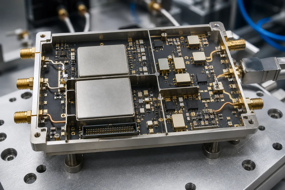
Representative product image. Confirm appearance and specifications with the manufacturer.

Product Specifications

Technical details and manufacturing context for RF Transceiver Module

Definition
The RF Transceiver Module is a critical component of a Cellular Modem responsible for modulating, transmitting, receiving, and demodulating radio frequency signals. It serves as the primary interface between the modem's digital baseband processor and the cellular network's antenna, enabling wireless data communication over specific cellular frequency bands (e.g., 4G LTE, 5G). The module integrates transmitter and receiver sections, along with associated circuitry, in a compact package suitable for space-constrained applications. It is designed to operate within defined frequency ranges, output power levels, and receiver sensitivity thresholds, as specified by industry standards such as 3GPP TS 36.101. The module's performance parameters, including frequency range (700–2700 MHz), output power (23–33 dBm), receiver sensitivity (-108–-98 dBm), supply voltage (3.3–4.2 V), operating temperature (-40–85 °C), and modulation support (QPSK–256QAM), are typical reference values that must be verified for the specific model and application. The module interfaces with the baseband processor via a control interface (MIPI RFFE) and is housed in a package typically sized 5.5–7.0 mm, with a weight of 0.5–1.5 g. Materials used include silicon for integrated circuits, ceramic substrate, gold/copper traces, solder, and plastic/metal housing. The module's insertion loss (1.5–3.0 dB) and noise figure (1.5–3.5 dB) are important for signal integrity. Harmonic suppression relative to carrier is -30 to -20 dBc. These parameters are provided as directory reference ranges and must be confirmed with the legal manufacturer or supplier for the actual model. The module is intended for use in cellular modems and similar wireless communication devices, and its selection should consider the specific frequency bands, power requirements, and environmental conditions of the application.
Working Principle
The module operates by receiving digital data from the modem's baseband processor. A transmitter section converts this data into an analog radio frequency signal, amplifies it, and sends it to the antenna for broadcast. Conversely, the receiver section captures incoming RF signals from the antenna, amplifies and filters them, then converts them back into digital data for the baseband processor to interpret. The module's operation is controlled via the MIPI RFFE interface, allowing configuration of frequency, power, and other parameters. The module's performance is characterized by parameters such as insertion loss and noise figure, which affect signal quality. The module is designed to operate within specified temperature and voltage ranges, and its harmonic suppression ensures compliance with spectral emission requirements.
Common Materials
Silicon (for integrated circuits), Ceramic Substrate, Gold/Copper Traces, Solder, Plastic/ Metal Housing
Technical Parameters
ParameterTypical rangeNotes & selection driver
Frequency Range700–2700 MHzCovers LTE/5G NR bands3GPP TS 36.101
Output Power23–33 dBmClass 3 typical, Class 2 for high power3GPP TS 36.101
Receiver Sensitivity-108–-98 dBmHigher sensitivity for low data rates3GPP TS 36.101
Supply Voltage3.3–4.2 VTypical Li-ion battery range
Operating Temperature-40–85 °CIndustrial gradeIEC 60068-2-1/2
InterfaceMIPI RFFEControl interface for configurationMIPI Alliance
Modulation SupportQPSK–256QAMHigher order for LTE/5G3GPP TS 36.101
Insertion Loss1.5–3.0 dBIn TX path, affects efficiency
Noise Figure1.5–3.5 dBLower is better for sensitivity
Package Size5.5–7.0 mmQFN package typicalJEDEC MO-220
Weight0.5–1.5 gIncluding shielding
Harmonic Suppression-30–-20 dBcRelative to carrier3GPP TS 36.101

Ranges are indicative industry figures for RFQ preparation, not a supplier commitment. Confirm every value and standard with the legal manufacturer before ordering.

Components / BOM
  • Power Amplifier (PA)
    Amplifies the low-power RF signal from the modulator to a level suitable for transmission via the antenna.
    Material: Gallium Arsenide (GaAs) or Silicon Germanium (SiGe) semiconductor
  • Low-Noise Amplifier (LNA)
    Amplifies the weak received RF signal from the antenna while adding minimal electronic noise.
    Material: Silicon or GaAs semiconductor
  • RF Filter/Duplexer
    Filters out-of-band interference and, in FDD systems, separates transmit and receive frequencies to allow simultaneous operation.
    Material: Ceramic (SAW/BAW filters) or Metal Cavities
  • RF Switch
    Routes RF signals between different paths, such as selecting between multiple antennas or frequency bands.
    Material: Silicon-on-Insulator (SOI) or GaAs semiconductor
  • Analog Signal Converter
    Converts baseband data to an analog RF signal for transmit, and back to digital on receive.
  • MIPI RFFE Interface
    The control port through which frequency, power and band are configured.

Applied To / Applications

This component is essential for the following industrial systems and equipment:

Industrial Ecosystem & Supply Chain Structure

Complementary Systems
Downstream Applications
Specialized Tooling

Application Fit & Sizing Matrix

Operational Limits
voltage: 3.0V to 3.6V
temperature: -40°C to +85°C
output power: Up to +23 dBm
frequency range: 400 MHz to 6 GHz
receiver sensitivity: -110 dBm typical
Media Compatibility
✓ Cellular networks (LTE, 5G NR) ✓ IoT communication systems ✓ Wireless sensor networks
Unsuitable: High-vibration industrial machinery without proper shock mounting
Sizing Data Required
  • Required frequency bands and bandwidth
  • Desired data rate and modulation scheme
  • Antenna gain and link budget requirements

Reliability & Engineering Risk Analysis

Failure Mode & Root Cause
Thermal stress-induced solder joint fatigue
Cause: Cyclic thermal expansion/contraction from power cycling or environmental temperature fluctuations, leading to micro-cracks in solder connections, especially with lead-free solder and mismatched coefficients of thermal expansion (CTE) between components and PCB.
RF signal degradation due to component drift or contamination
Cause: Aging or environmental exposure causing parameter shifts in oscillators, filters, or amplifiers (e.g., capacitor dielectric absorption, inductor core saturation), or contamination (dust, moisture) on RF paths increasing insertion loss and impedance mismatches.
Maintenance Indicators
  • Intermittent or complete loss of signal transmission/reception despite proper power and configuration, often accompanied by increased bit error rates (BER) or dropped connections.
  • Abnormal thermal patterns detected via infrared imaging, such as localized overheating on specific ICs (e.g., power amplifiers) or unexpected cold spots indicating component failure.
Engineering Tips
  • Implement controlled thermal management: Use conformal coatings to buffer thermal cycling, ensure adequate heatsinking/ventilation for high-power components, and design with CTE-matched materials to reduce mechanical stress on solder joints.
  • Establish preventive calibration and environmental sealing: Schedule periodic RF performance verification (e.g., VSWR, output power tests) to detect early drift, and seal modules in enclosures with desiccants or gaskets to protect against moisture, dust, and corrosive contaminants.

Indicative industry ranges for design and RFQ preparation. Confirm the exact figures and applicable standard with the manufacturer before specifying.

Compliance & Manufacturing Standards

Applicable Standards
CE Marking (EU Directive 2014/53/EU for Radio Equipment) ANSI C63.4:2014 Methods of Measurement of Radio-Noise Emissions from Low-Voltage Electrical and Electronic Equipment

Quoted from the published standard.

Manufacturing Precision
  • Frequency Stability: +/- 2.5 ppm
  • Output Power Variation: +/- 1.5 dB
Quality Inspection
  • Spectrum Analyzer Test for RF Performance
  • Environmental Stress Screening (ESS) for Reliability

Manufacturers of RF Transceiver Module

Manufacturer profiles associated with RF Transceiver Module.

Sourcing RF Transceiver Module from China?
Tell us your specification and target quantity — we will match it against manufacturer records and come back with the factories that fit.
Request manufacturers We manufacture this

Manufacturer listings support early research and capability understanding. They are not certification, ranking, or transaction guarantees.

Technical documentation
Request current drawings, revision history, and a signed specification sheet.
Manufacturing capability
Verify equipment lists, process limits, capacity, and representative production evidence.
Inspection readiness
Confirm test methods, calibrated equipment, sampling plans, and traceable reports.
Supplier transparency
Check the legal entity, factory address, ownership, certifications, and direct contacts.

CNFX does not score or rank suppliers. Buyers must verify all claims and documents with the legal manufacturer before ordering.

Supply Chain Compatible Machinery & Devices

Modular Industrial Edge Computing Device

This modular industrial edge computing device is a ruggedized system designed for deployment in harsh industrial environments to perform real-time data processing, analytics, and control functions at the network edge.

Explore Specs →
Industrial Smart Camera Module

The Industrial Smart Camera Module is a compact, self-contained vision processing unit designed for integration into industrial machinery and production lines.

Explore Specs →
Surface Mount Resistor

Passive electronic component for current limiting and voltage division in circuits

Explore Specs →
Surface Mount Capacitor

A surface mount capacitor is a fundamental electronic component used for energy storage, filtering, coupling, and decoupling in electronic circuits.

Explore Specs →

Frequently Asked Questions

What is the typical frequency range of this RF transceiver module?

The directory reference lists a frequency range of 700–2700 MHz, covering LTE and 5G NR bands. However, the actual supported bands depend on the specific model and must be confirmed with the manufacturer.

What is the output power capability?

The reference output power is 23–33 dBm, with Class 3 typical and Class 2 for high power. Actual output power varies by model and configuration, so verify with the supplier.

What is the receiver sensitivity?

The reference receiver sensitivity is -108 to -98 dBm, with higher sensitivity for low data rates. Confirm the exact sensitivity for your application with the manufacturer.

What standards apply to this module?

The module references standards such as 3GPP TS 36.101 for RF performance and MIPI RFFE for the control interface. These are verification references, not proof of certification. Always check compliance with the manufacturer.

Data Basis

Editorial classification, named public sources where available, and source-reviewed manufacturer records.

Preliminary Technical Classification
This page supports structured research, RFQ preparation, and supplier evaluation. It does not replace buyer-led supplier qualification, standards review, or technical approval.
Buyer enquiry

Request manufacturing insight for RF Transceiver Module

Ask for use case, specification boundaries, supplier type, and RFQ preparation information for this product.

Where it goes
Straight to the CNFX editorial desk, and to the manufacturer if this product is linked to a claimed profile. Nothing is broadcast to a supplier list.
Your details stay here
We do not sell or rent enquiry data, and we do not add you to a mailing list. Used only to answer this request.
No commission, no middleman
CNFX is a directory. We take no cut of any order and never negotiate on a supplier's behalf.
What we don't claim
A listing is not an endorsement. Qualify every supplier and verify every figure yourself before ordering.

Your business information is used only to process this request.

Thank you! Your message has been sent. We'll respond within 1–3 business days.
Sorry, we couldn't send your message. Please try again, or email us at contact@cnfx.com.

Need to Manufacture RF Transceiver Module?

Compare manufacturer profiles with relevant product and process capability.

Previous Product
XY Positioning Stage
Last Product
Get QuotesChat