Photodiode photodetectors · Photosensitivity and quantum efficiency, NEP and linearity, rise time set by capacitance and load, bandwidth
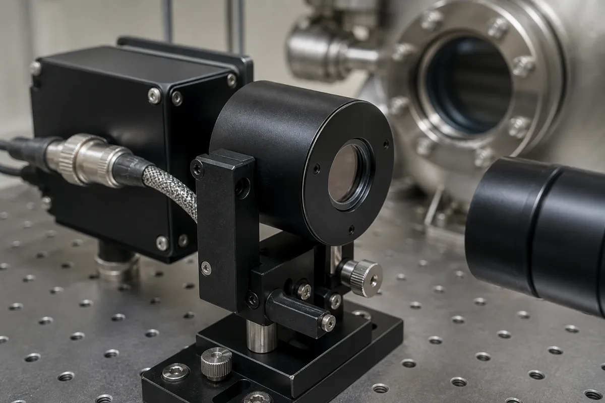
A photodetector converts light into an electrical signal; the photodetectors on this page use a photodiode, alone or with a built-in amplifier in a housed module like the one pictured on an optical bench. Ask three things first: what photosensitivity (A/W) the detector has at your wavelength, what noise equivalent power and linear range it offers for your light level, and what bandwidth it reaches with the capacitance, bias and load or amplifier you will use.
Photodiode-based photodetectors: PIN and avalanche photodiodes, amplified photodetector modules, fibre-coupled and balanced photodetectors. Image sensors and cameras, photomultiplier tubes, thermal detectors and complete optical receivers or transceivers are outside this page.
CNFX editorial research · Sources checked October 12, 2026 · 4 sources
Check photosensitivity, quantum efficiency, noise and linearity
Hamamatsu's technical note on Si photodiodes defines quantum efficiency as photocurrent electrons per incident photon, QE = S × 1240 ÷ λ × 100%, with S the photosensitivity in A/W and λ the wavelength in nm. It defines noise equivalent power (NEP) as the light level giving a current equal to the noise current, NEP = noise current ÷ S, in W/Hz½, and says photocurrent is linear over more than nine orders of magnitude, from about 10⁻¹² to 10⁻² W depending on the device and circuit, with the upper limit set by load resistance and reverse voltage. [1]
Hamamatsu's datasheet for its S5971, S5972 and S5973 Si PIN photodiodes gives peak photosensitivity of 0.64 A/W at 920 nm (S5971), 0.57 A/W at 800 nm (S5972) and 0.52 A/W at 760 nm (S5973), dark currents of 0.07 nA, 0.01 nA and 0.001 nA (typ.), and NEPs of 7.4, 3.1 and 1.1 × 10⁻¹⁵ W/Hz½; the violet-enhanced S5973-02 reaches 0.3 A/W and 91% QE at 410 nm. [2]
Editorial calculation: the QE formula reproduces the datasheet figure, 0.3 × 1240 ÷ 410 ≈ 91%; for the S5971 at its 920 nm peak, 0.64 × 1240 ÷ 920 ≈ 86%. Compare detectors at the wavelength you will use, not at each one's peak.
An avalanche photodiode adds internal gain. Excelitas' C30902SH silicon reach-through APD (data sheet Rev. 2022.02) has a 0.5 mm active diameter, 400–1,100 nm response and 84% quantum efficiency at 800 nm. In linear mode at its recommended gain of 250 it lists responsivity as 117 and 135 A/W, 0.4 ns rise and fall time, 800 MHz bandwidth, capacitance as 1.5 and 1.8 pF (the extracted table does not show which of its three columns each of these two figures belongs to; confirm with Excelitas), dark current of 7 nA (typ.) and 10 nA maximum, and NEP of 0.74 fW/√Hz, falling to 0.29 and 0.15 fW/√Hz with one- and two-stage thermo-electric coolers. [3] Breakdown voltage is 185–260 V (225 V typ.) with a temperature coefficient of 0.5–0.9 V/°C, and it can also run above breakdown in Geiger mode to count single photons. [3]
Editorial calculation: dividing the APD's 135 A/W by its gain of 250 gives a unity-gain responsivity of about 0.54 A/W at 800 nm, close to a PIN photodiode's; the APD's advantage is gain ahead of the amplifier noise. Excelitas gives a breakdown temperature coefficient of 0.7 V/°C (typ.) [3]; at that value a 10 °C rise moves breakdown by about 7 V, so gain must be held by bias or temperature control.
Give the supplier the wavelength range, optical power range, required bandwidth or rise time, free-space or fibre input (fibre type and connector), active area, output (current, voltage, amplified gain), noise requirement, single or balanced detection, supply, operating temperature and mounting.
02
Work out rise time and bandwidth from capacitance and load
Hamamatsu's note explains that rise time (10% to 90%) depends on three factors: the time constant of terminal capacitance and load resistance, t₁ = 2.2 × Ct × RL; the diffusion time of carriers generated outside the depletion layer, which can run to microseconds; and carrier transit time in the depletion layer. Rise time is approximately √(t₁² + t₂² + t₃²), and cutoff frequency fc ≈ 0.35 ÷ tr. Applying reverse voltage reduces capacitance and speeds response but increases dark current. [1]
The S5971, S5972 and S5973 series reach cutoff frequencies of 0.1 GHz and 0.5 GHz at 10 V reverse bias and 1 GHz at 3.3 V, with terminal capacitance of 3 pF (S5971/S5972, 10 V) and 1.6 pF (S5973, 3.3 V); photosensitive areas are 1.2, 0.8 and 0.4 mm diameter, and the maximum reverse voltage is 20 V. [2]
Editorial calculation: with Ct = 3 pF into a 50 Ω load, t₁ = 2.2 × 3 pF × 50 Ω ≈ 0.33 ns, a capacitance limit of about 1 GHz; into a 10 kΩ load, t₁ ≈ 66 ns and fc ≈ 5 MHz. Larger load resistance or amplifier gain raises signal but cuts bandwidth, so state the bandwidth at the gain you need. [1]
A single InGaAs product family shows active area trading against speed. OSI Optoelectronics lists its FCI-InGaAs series in TO-18 packages with the same responsivity, 0.9 A/W at 1310 nm and 0.95 A/W at 1550 nm, across four active-area diameters, while capacitance, dark current and rise time all rise with area. [4]
Editorial calculation: values in the first five columns are from OSI [4]; the last column applies Hamamatsu's fc ≈ 0.35 ÷ rise time [1]. Going from the 75 µm to the 500 µm device raises capacitance 13-fold and rise time 50-fold. Using Hamamatsu's QE formula, 0.95 A/W at 1550 nm is a quantum efficiency of 0.95 × 1240 ÷ 1550 ≈ 76%, and 0.9 A/W at 1310 nm is about 85%. [4][1]
OSI FCI-InGaAs model
Active area diameter
Dark current
Capacitance
Rise time
Editorial: fc ≈ 0.35 ÷ rise time
FCI-InGaAs-75
75 µm
0.03 nA
1.5 pF
0.2 ns
≈ 1.75 GHz
FCI-InGaAs-120
120 µm
0.05 nA
2 pF
0.3 ns
≈ 1.17 GHz
FCI-InGaAs-300
300 µm
0.30 nA
10 pF
1.5 ns
≈ 233 MHz
FCI-InGaAs-500
500 µm
0.5 nA
20 pF
10 ns
≈ 35 MHz
03
PIN, APD, balanced and 10 Gbps modules in the listings
Listings include PIN, avalanche (APD), amplified and balanced photodetectors and high-speed 10 Gbps modules for fibre systems, offered alongside lasers, modulators and fibre sensing equipment. Ask each supplier for responsivity at your wavelength, NEP, bandwidth at the stated gain, saturation power and the fibre or free-space input.
04
Photodiode, window, bias, amplifier and package
The bias row works differently for the two detector types on this page: reverse voltage on a PIN photodiode lowers capacitance at the cost of more dark current, while an APD is biased near its breakdown voltage. [1][3]
Photodetector module sources and what else they make
Rofea and YB Photonics list PIN, APD and balanced photodetectors, the first with modulators and the second with fibre sensing systems; Box Optronics lists photodetectors next to DFB lasers and SLED modules.
Beijing Rofea Optoelectronics Co., Ltd.
Manufacturing site to be confirmed for the order
Lists PIN, APD, balanced and high-speed photodetector modules with modulators.
Explore company information and manufacturing capabilities, then discuss the scope of your project with a relevant supplier.
Share this page
Compiled and source-reviewed by the CNFX editorial team.
Each manufacturer above links to the page on that company's own website where the product is listed, with the date we checked it. How we source and review
· Page last updated 13 October 2026
Buyer questions
How do I convert A/W into quantum efficiency?
Hamamatsu gives QE = S × 1240 ÷ λ × 100%; 0.3 A/W at 410 nm is about 91%. [1][2]
What limits photodetector bandwidth?
Hamamatsu cites the capacitance-load time constant (t₁ = 2.2 Ct RL), carrier diffusion and transit times, with fc ≈ 0.35 ÷ rise time. [1]
What is NEP?
Hamamatsu defines it as the light level whose photocurrent equals the noise current, noise current divided by photosensitivity, in W/Hz½. [1]
How much responsivity does an avalanche photodiode add?
Excelitas' C30902SH gives 117–135 A/W at a gain of 250 and 800 nm, with 800 MHz bandwidth and 0.74 fW/√Hz NEP. [3]
Does a larger photodiode area slow the detector?
In OSI's FCI-InGaAs series, the 75 µm device has 1.5 pF and 0.2 ns rise time while the 500 µm device has 20 pF and 10 ns, at the same 0.95 A/W at 1550 nm. [4]
Sources and what still needs a direct check
Sources checked 2026-10-12. Hamamatsu Photonics, Excelitas Technologies and OSI Optoelectronics are photodetector makers; Hamamatsu's technical note explains photodiode characteristics, and each datasheet or product table gives values for that maker's own devices.