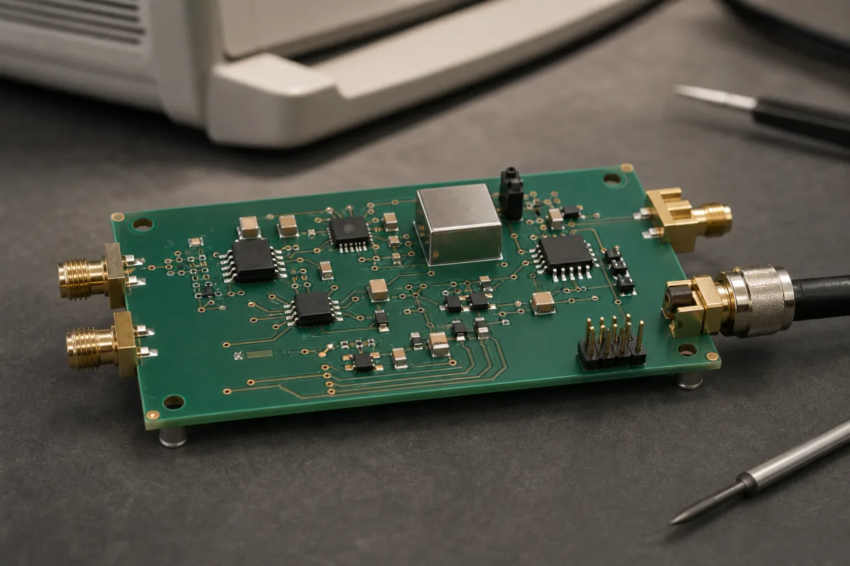
Sample-and-hold ICs · Acquisition time vs hold capacitor, droop from leakage, hold step from charge coupling, gain accuracy and offset, feedthrough, logic input and supplies
A sample-and-hold (track-and-hold) circuit follows an analog input and, on a logic command, freezes its value on a hold capacitor so an ADC, comparator or control loop can use a steady voltage. Settle three things before choosing one: the acquisition time and the hold capacitor that set speed, the droop, hold step and feedthrough that set error during hold, and the accuracy, input and output impedance, logic interface, supplies and package.
Monolithic sample-and-hold and track-and-hold ICs and the hold-capacitor choice around them. ADCs with built-in sampling, peak detectors, analog switches and multiplexers sold alone are outside this page; ADC chips have their own page.
CNFX editorial research · Sources checked October 12, 2026 · 5 sources
TI's LF198-N/LF298/LF398-N datasheet describes monolithic sample-and-hold circuits using BI-FET technology for high DC accuracy, fast acquisition and low droop. Operating as a unity-gain follower, DC gain accuracy is 0.002% (typ.) and acquisition time is as low as 6 µs to 0.01%; input impedance of 10¹⁰ Ω allows high source impedances, and the bandwidth allows use inside the loop of 1 MHz op amps. [1]
The electrical characteristics list acquisition time to 0.1% for a 10 V step of 4 µs with a 1,000 pF hold capacitor and 20 µs with 0.01 µF, with 5 mA hold-capacitor charging current; supply current of 4.5 mA (typ.); and operation from ±5 V to ±18 V. Logic inputs are fully differential with a 1.4 V threshold for direct connection to TTL, PMOS and CMOS. [1]
Faster parts integrate the hold capacitor. Renesas' HA-5320 is a precision sample-and-hold amplifier with a transconductance input stage, a low-leakage switch working into virtual ground and an integrating output amplifier with an internal hold capacitor; it lists 1.0 µs acquisition to 0.01%, 25 ns aperture time, DC gain of 2 × 10⁶ V/V, fully differential inputs and TTL-compatible control, and allows external hold capacitance to be added when lower droop is worth slower acquisition. Renesas' HA-5340 combines an integrating output with a buffered hold capacitor to reach 700 ns acquisition and 200 ns hold-mode settling to 0.01%, with a built-in 135 pF hold capacitor and bandwidth only minimally affected by added capacitance. [2][3]
Editorial note: a larger hold capacitor lowers droop and hold step but lengthens acquisition, so choose it from the shortest sample window you must meet and the longest hold you need. [1]
Give the supplier the input range and source impedance, acquisition time to the accuracy you need, hold time and allowed droop, hold step, feedthrough limit, gain accuracy and offset, logic levels, supply rails, temperature range, package, and the hold-capacitor type you intend to use.
02
Limit droop, hold step and feedthrough
The LF198-N/LF298 table lists leakage into the hold capacitor of 30 pA (typ.), 100 pA maximum, at 25 °C, giving droop rates as low as 5 mV/min with a 1 µF capacitor; hold step of 0.5 mV (typ.), 2 mV maximum, at 0.01 µF; feedthrough attenuation of 86 dB minimum and 96 dB (typ.) at 1 kHz with 0.01 µF; output impedance of 0.5 Ω (typ.), 2 Ω maximum, in hold; and supply rejection of 80 dB minimum, 110 dB (typ.). It notes that hold step is sensitive to stray capacitance between the logic inputs and the hold capacitor — 1 pF adds about 0.5 mV with a 5 V logic swing and 0.01 µF — and that hold step is inversely proportional to hold capacitance. [1]
Editorial calculation: droop ≈ leakage ÷ capacitance, so 30 pA into 0.01 µF is about 3 mV/s, and into 1 µF about 0.03 mV/s (1.8 mV/min); scaling the 0.5 mV hold step at 0.01 µF inversely gives about 0.05 mV at 0.1 µF. [1]
The HA-5320 lists droop of 0.08 µV/µs at 25 °C and 17 µV/µs over full temperature and a hold step error of 5 mV, which can be nulled through its offset-adjust inputs because the charge injection is constant across the input range. The HA-5340 lists hold-mode distortion of −72 dBc for a 200 kHz, 5 Vp-p input sampled at 450 kHz, and a constant pedestal error that can likewise be nulled. [2][3]
Editorial calculation: the HA-5320's 0.08 µV/µs droop at 25 °C equals 0.08 V/s, but its full-temperature figure of 17 µV/µs is over 200 times higher (17 ÷ 0.08), so hold times must be checked at the hottest operating point. [2]
Editorial note: keep logic traces away from the hold capacitor and guard it, because the datasheet ties part of the hold step directly to stray coupling. [1]
03
Pick the hold-capacitor dielectric for low absorption and leakage
Film-capacitor maker WIMA explains that a capacitor charged for a long time and then fully discharged shows a small voltage on its terminals again within seconds or minutes — dielectric absorption — and that this effect is particularly unfavourable in sample-and-hold circuits. It describes the MIL-C-19978 measurement: charge for 15 minutes, discharge through 50 Ω for 10 s, then read the regained voltage after 15 minutes with a meter above 10,000 MΩ; dielectric absorption is regained voltage divided by charged voltage. [4]
WIMA lists sample and hold among the applications for its polypropylene capacitors, with insulation resistance falling to 10,000 MΩ × µF at 85 °C, and it gives polypropylene film thickness as more than 4 µm and a maximum working temperature of +105 °C. [5]
Editorial calculation: a 0.01 µF polypropylene capacitor at 100,000 MΩ × µF has 10¹³ Ω insulation resistance, so 10 V across it leaks about 1 pA, against the LF398-N's 30 pA (typ.) hold-capacitor leakage; the same value in X7R at 1,000 MΩ × µF leaks about 100 pA. Dielectric absorption of 0.05–0.10% on a 10 V step corresponds to 5–10 mV in the MIL-C-19978 test, against 2.00–2.50% (200–250 mV) for Z5U. Ask the supplier which hold-capacitor dielectric its acquisition and droop figures assume. [4][5][1]
Dielectric
Dielectric absorption at 23 °C (%)
Insulation resistance × capacitance at 25 °C (MΩ × µF)
External-capacitor LF398 versus internal-capacitor HA-5320 and HA-5340
The reviewed data sheets cover a general-purpose BI-FET sample-and-hold with an external hold capacitor (LF398) and fast dielectrically isolated sample-and-hold amplifiers with internal hold capacitors for data acquisition, DAC deglitching and peak detection (HA-5320, HA-5340). [1][2][3]
Ask any supplier for acquisition time, droop and hold step at your hold capacitor and temperature. [1]
05
Input amplifier, switch, hold capacitor and output amplifier
On the LF398 the hold capacitor sits outside the chip, so its value and dielectric are the buyer's choice; the HA-5320 and HA-5340 build one in. [1][2][3]
Acquisition time, aperture, droop, gain error and hold time for a sample-and-hold order
Acquisition time and droop both move with the hold capacitor, so ask for them at your Ch value; aperture jitter, temperature range and the signal and hold-time rows have no published value here and come from the supplier or your design. [1]
Field
What it means and published values
Ask the supplier for
Acquisition Time
4 µs (1,000 pF); 20 µs (0.01 µF) to 0.1%. [1] Also 700 ns–1.0 µs to 0.01%. [3][2]
At your Ch.
Aperture Delay
Command-to-hold delay. E.g. 25 ns aperture time. [2]
ns.
Aperture Jitter
Timing uncertainty.
ps rms.
Hold Capacitance
External; 1,000 pF to 1 µF in examples. [1] E.g. built-in 135 pF. [3]
Recommended value.
Droop Rate
As low as 5 mV/min with 1 µF. [1] E.g. 0.08 µV/µs at 25 °C. [2]
Explore company information and manufacturing capabilities, then discuss the scope of your project with a relevant supplier.
Share this page
Compiled and source-reviewed by the CNFX editorial team.
Each manufacturer above links to the page on that company's own website where the product is listed, with the date we checked it. How we source and review
· Page last updated 13 October 2026
Buyer questions
What sets sample-and-hold acquisition time?
The hold capacitor value is one factor; for a 10 V step settling to 0.1%, TI lists 4 µs with 1,000 pF and 20 µs with 0.01 µF for the LF398-N. [1]
What causes droop in a sample-and-hold?
Leakage into the hold capacitor; TI lists 30 pA (typ.) and droop as low as 5 mV/min with 1 µF. [1]
What is hold step?
The output jump when switching to hold; TI lists 0.5 mV (typ.) at 0.01 µF for the LF198-N/LF298 (1 mV for the LF398-N) and says it is inversely proportional to capacitance. [1]
How accurate is a sample-and-hold?
TI's datasheet gives gain error of 0.002% (typ.) for the LF198-N and LF298 and 0.004% (typ.) for the LF398-N, as unity-gain followers at 25 °C. [1]
How fast can a sample-and-hold amplifier acquire a signal?
Published parts range from 4–20 µs with an external capacitor to 700 ns–1 µs to 0.01% for amplifiers with internal hold capacitors. [1][2][3]
Which capacitor dielectric suits a sample-and-hold?
WIMA lists dielectric absorption of 0.05–0.10% for polypropylene, 0.20–0.25% for polyester, 0.60–1.00% for X7R and 2.00–2.50% for Z5U ceramic, and names sample and hold as a polypropylene application. [4][5]
Sources and what still needs a direct check
Sources checked 2026-10-12. Texas Instruments publishes the LF198-N/LF298/LF398-N monolithic sample-and-hold datasheet; Renesas publishes the HA-5320 and HA-5340 data sheets; film-capacitor maker WIMA publishes dielectric absorption and insulation-resistance data for hold-capacitor dielectrics.