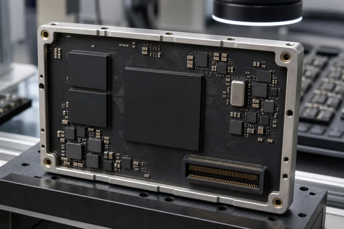
Baseband processor for 5G NR user equipment: the modem chip whose layers, modulation order and aggregated carriers set its 3GPP peak rate and its layer 2 buffer
5G NR modem chips · the 3GPP TS 38.306 peak-rate formula behind a "10 Gbps" claim, the layer 2 buffer the rate forces on modem memory, and two published modem chips compared
The baseband processor is the digital half of a cellular modem: it runs the physical layer, the protocol stack and the carrier aggregation logic, while separate RF transceivers and front-end modules handle the radio signal. When a modem chip is sold as "up to 10 Gbps", that number is a capability calculation defined by 3GPP, not a measured link speed. The same calculation decides how much layer 2 buffer memory the chip must hold, and the band combinations it supports decide whether that number is reachable on a given network.
Baseband processors (5G NR and LTE modem chips) for phones, fixed-wireless terminals and other user equipment, read through their 3GPP capability: peak data rate per TS 38.306, carrier aggregation, MIMO layers and modulation order, layer 2 buffer, and the host interface. RF integrated circuits that handle the radio signal itself are covered on the RF integrated circuits (RFICs) page; board-level transceiver layout on the RF Transceiver page; PA, LNA and switch assemblies on the RF Front-End Module page; complete serial-to-cellular terminals on the Cellular modem page. Base-station (RAN) baseband units are outside this page.
CNFX editorial research · Sources checked October 13, 2026 · 5 sources
The TS 38.306 peak-rate formula: layers, modulation order, scaling factor, PRBs and overhead per component carrier
3GPP TS 38.306 clause 4.1.2 defines the approximate NR data rate as a sum over the J aggregated component carriers of a band or band combination. For each carrier it multiplies the number of MIMO layers, the modulation order Qm, a scaling factor f (1, 0.8, 0.75 or 0.4), the maximum code rate Rmax = 948/1024, and the number of resource blocks times 12 subcarriers divided by the average OFDM symbol time, then removes an overhead share. A UE "shall support" the rate this calculation gives. [1]
Editorial calculation with example values (not a figure from any chip maker): one 100 MHz FR1 carrier at 30 kHz (μ = 1, so T_s = 35.7 µs and N_PRB = 273), with 4 downlink layers, 256-QAM (Qm = 8) and f = 1, gives 4 × 8 × 0.926 × 273 × 12 / 35.7 µs × (1 − 0.14) ≈ 2,337 Mbps. The same carrier with 2 uplink layers, 256-QAM and the 0.08 FR1 uplink overhead gives about 1,250 Mbps. [1][2]
The formula is a sum over carriers, so a downlink figure larger than one carrier's result can only come from aggregating carriers, from FR2 bandwidths, or from both. For a single carrier in NR standalone operation, TS 38.306 also sets a floor: the product of layers, modulation order and scaling factor must be no smaller than 4, for example one layer with Qm = 4 and f = 1. [1] For EUTRA carriers in dual connectivity the rate is instead the sum of transport-block bits per 1 ms TTI, and in MR-DC the LTE and NR results are added. [1]
Term in TS 38.306 4.1.2
What sets it
v (layers)
maxNumberMIMO-LayersPDSCH for downlink; the larger of the codebook and non-codebook PUSCH layer limits for uplink [1]
Ask the chip supplier for the band combinations behind its headline rate: per carrier, the band, bandwidth, SCS, layers, modulation order and scaling factor, so the rate can be recomputed with the TS 38.306 formula.
02
How much layer 2 memory a modem needs: peak rate multiplied by the RLC round trip of 20 to 75 ms
TS 38.306 clause 4.1.4 defines the total layer 2 buffer as the bytes the UE must hold in its RLC transmission, reception and reassembly windows and its PDCP reordering windows for all radio bearers. Outside dual connectivity it is the maximum downlink rate times the RLC round-trip time plus the maximum uplink rate times the RLC round-trip time. [1]
The RTT used for an NR cell group is the one for the smallest SCS numerology in the band combination, and the buffer required is the maximum over every supported band combination and feature-set combination; TS 38.306 adds that memory used for pre-processing data is not included. [1]
Editorial calculation using the example carrier above (example values, 30 kHz, 40 ms RTT): (2,337 + 1,250 Mbps) × 0.040 s ≈ 143 Mbit, about 18 MB of layer 2 buffer for that single carrier. In MR-DC the formula adds the inter-node delay of 25 or 55 ms to one leg, so an LTE-anchored combination asks for more buffer at the same rate. [1] This is one reason a modem's memory interface and its supported band combinations belong in the same review.
25 ms if the other cell group is NR, 55 ms if it is EUTRA [1]
Request the UE capability set (band combinations and feature sets) the chip reports, the resulting layer 2 buffer figure, and whether that buffer sits in on-chip memory or in external DRAM on the module.
03
Exynos Modem 5300 and MediaTek M80: what two modem makers publish about rate, carriers, process and host link
Both makers publish headline rates without the band combination behind them, so the figures below are their statements and cannot be recomputed from the pages alone. [3][4]
Samsung notes that its product specifications reflect internal test results and vary with the user's system configuration. [3] Editorial calculation: Samsung's 10 Gbps is about 4.3 times the 2,337 Mbps example carrier above, so it cannot be reached on one 100 MHz FR1 carrier with 4 layers and 256-QAM; Samsung's page does not state which FR1/FR2 combination produces it. [3][1]
For a design-in, ask each modem supplier for the reference design (RF transceiver, front-end and antenna parts it was certified with), the operator and regulatory certifications obtained, the host interface (PCIe generation and lanes), and the band combination list for your target markets.
04
What to send a modem chip supplier
Paste it into your enquiry below or into an email to a maker, then replace every bracket.
Device: [phone, FWA terminal, module, other]
Networks: [5G SA/NSA; LTE; legacy RATs; target operators]
Bands: [FR1 and FR2 bands; required band combinations]
Rate targets: [DL/UL per band combination; layers; modulation]
Host: [application processor; PCIe or other interface]
Memory: [layer 2 buffer; on-chip or external DRAM]
Release: [3GPP release; features such as VoNR, DSS, dual SIM]
Documents: [UE capability list; reference design; certifications]
Explore company information and manufacturing capabilities, then discuss the scope of your project with a relevant supplier.
Share this page
Compiled and source-reviewed by the CNFX editorial team.
Each manufacturer above links to the page on that company's own website where the product is listed, with the date we checked it. How we source and review
· Page last updated 13 October 2026
Buyer questions
How is a 5G modem's peak data rate calculated?
3GPP TS 38.306 clause 4.1.2 sums, over the aggregated carriers, layers × modulation order × scaling factor × 948/1024 × (PRBs × 12 / symbol time) × (1 − overhead), with overhead 0.14 for FR1 downlink. [1]
How many resource blocks does a 100 MHz 5G carrier have?
TS 38.101-1 Table 5.3.2-1 gives 273 resource blocks for a 100 MHz FR1 channel at 30 kHz subcarrier spacing. [2]
What is the layer 2 buffer of a 5G modem?
TS 38.306 defines it as the bytes held in RLC and PDCP windows, calculated as peak downlink and uplink rates times the RLC round-trip time, which is 40 ms for a 30 kHz NR cell group. [1]
What peak rates do current 5G modem chips claim?
Samsung lists the Exynos Modem 5300 at up to 10 Gbps download and 3.87 Gbps upload; MediaTek lists the M80 at 7.67 Gbps downlink and 3.76 Gbps uplink. [3][4]
Sources and what still needs a direct check
Sources checked 2026-10-13. Five sources from three publishers: two ETSI publications of 3GPP specifications (TS 38.306 for the peak-rate and buffer formulas, TS 38.101-1 for the resource-block table), Samsung Semiconductor's Exynos Modem 5300 product page, and MediaTek's M80 launch post and infographic.