Power Electronics Module
View system integration details
This page explains how Gate Driver Circuit is classified within Computer, Electronic and Optical Product Manufacturing. Technical values and manufacturer relationships are research references; confirm the current specification and supplier evidence for each order.
Electronic circuit that controls the switching of power semiconductor devices by providing appropriate gate signals.
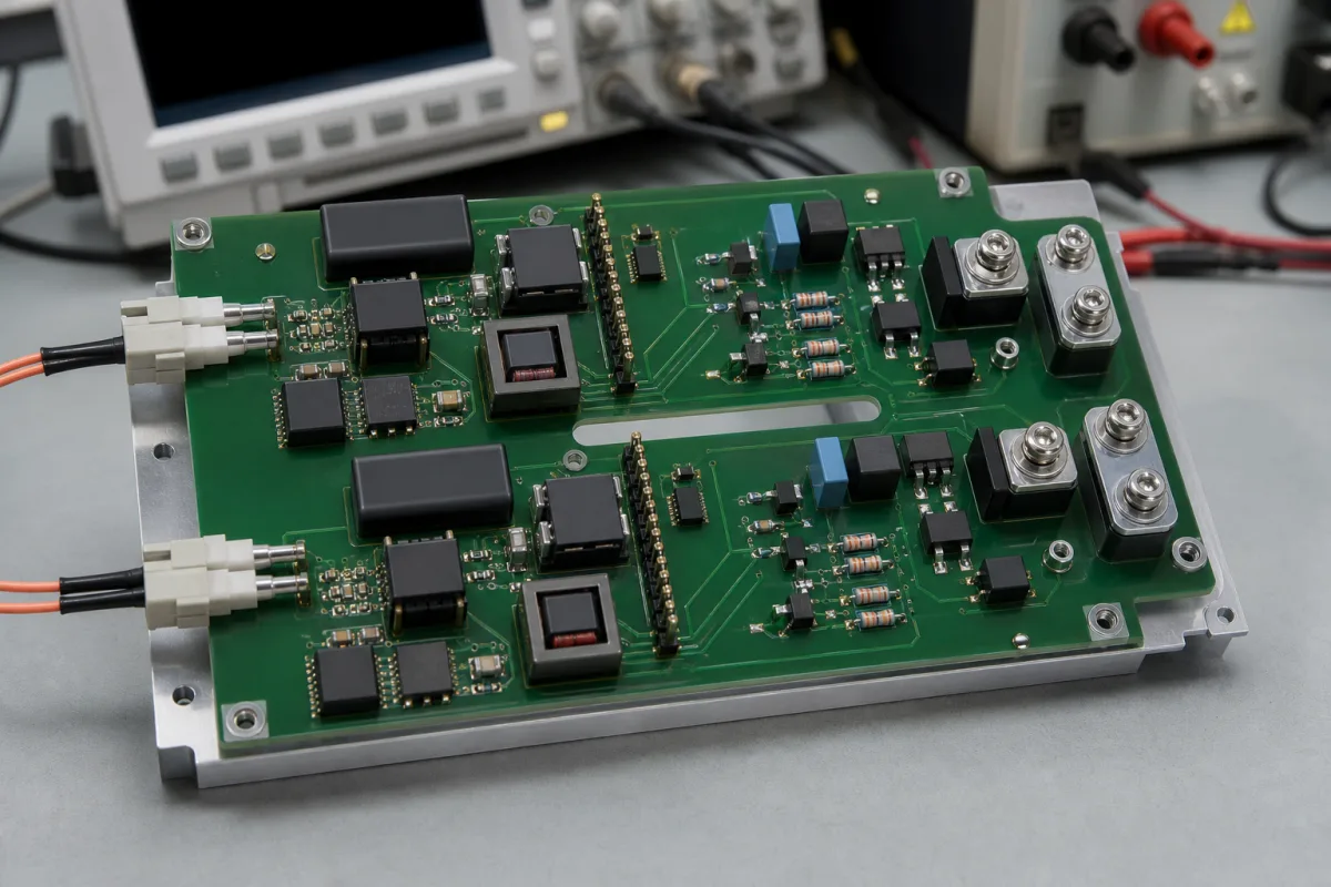
Technical details and manufacturing context for Gate Driver Circuit
| Parameter | Typical range | Notes & selection driver |
|---|---|---|
| Output Current (Peak) | 2–10 A | Determines gate charge capability |
| Output Voltage Swing | 10–30 V | Must match gate drive requirement |
| Switching Frequency | 100–500 kHz | Higher for SiC/GaN |
| Propagation Delay | 50–200 ns | Affects dead-time control |
| Rise/Fall Time | 10–50 ns | Minimizes switching losses |
| Supply Voltage | 10–30 V DC | Single or dual rail |
| Operating Temperature | -40–125 °C | Junction temperature limit |
| Isolation Voltage | 2.5–5 kVrms | For galvanic isolationIEC 60747 |
| CMTI (Common Mode Transient Immunity) | 50–100 kV/µs | Critical for high-side driving |
| Input Logic Level | 3.3–5 V | TTL/CMOS compatible |
| Package Type | SOIC-8–SOIC-16 | Footprint and thermal |
| Power Dissipation | 0.5–2 W | Thermal management |
Ranges are indicative industry figures for RFQ preparation, not a supplier commitment. Confirm every value and standard with the legal manufacturer before ordering.
| current: | Peak output current: 2A-10A typical |
| voltage: | Up to 1200V (isolation voltage), 5V-20V (gate drive voltage) |
| other spec: | Common-mode transient immunity: >50kV/μs, Propagation delay: <100ns typical |
| temperature: | -40°C to +125°C (operating), -55°C to +150°C (storage) |
| switching frequency: | Up to 1MHz (depending on topology and device) |
Indicative industry ranges for design and RFQ preparation. Confirm the exact figures and applicable standard with the manufacturer before specifying.
Quoted from the published standard.
A practical evidence checklist for RFQ preparation and supplier evaluation.
Compare the published product scope and source details, then include your specifications and quantity in an enquiry.
Manufacturer profiles associated with Gate Driver Circuit.
Explore company information and manufacturing capabilities, then discuss the scope of your project with a relevant supplier.
Ask for use case, specification boundaries, supplier type, and RFQ preparation information for this product.
A gate driver circuit amplifies low-power control signals from a microcontroller or PWM controller to the voltage and current levels needed to drive the gate of a power semiconductor device, ensuring efficient and reliable switching.
Key parameters include peak output current, output voltage swing, switching frequency, propagation delay, rise/fall time, supply voltage, operating temperature, isolation voltage, CMTI, input logic level, package type, and power dissipation. These must match the requirements of the power device and application.
Isolation protects low-voltage control circuitry from high-voltage transients in the power stage. It is achieved using optocouplers or transformers and is specified by isolation voltage ratings such as 2.5–5 kVrms.
Common protection features include under-voltage lockout (UVLO), desaturation detection, and short-circuit protection, which help prevent damage to the power device and the driver itself.
This component is essential for the following industrial systems and equipment:
Editorial classification, named public sources where available, and source-reviewed manufacturer records.
Compare manufacturer profiles with relevant product and process capability.